SPRACZ1 October 2021 F29H850TU , F29H859TU-Q1 , TMS320F280021 , TMS320F280021-Q1 , TMS320F280023 , TMS320F280023-Q1 , TMS320F280023C , TMS320F280025 , TMS320F280025-Q1 , TMS320F280025C , TMS320F280025C-Q1 , TMS320F280040-Q1 , TMS320F280040C-Q1 , TMS320F280041 , TMS320F280041-Q1 , TMS320F280041C , TMS320F280041C-Q1 , TMS320F280045 , TMS320F280048-Q1 , TMS320F280048C-Q1 , TMS320F280049 , TMS320F280049-Q1 , TMS320F280049C , TMS320F280049C-Q1 , TMS320F28044 , TMS320F28075 , TMS320F28075-Q1 , TMS320F28076 , TMS320F28374D , TMS320F28374S , TMS320F28375D , TMS320F28375S , TMS320F28375S-Q1 , TMS320F28376D , TMS320F28376S , TMS320F28377D , TMS320F28377D-EP , TMS320F28377D-Q1 , TMS320F28377S , TMS320F28377S-Q1 , TMS320F28378D , TMS320F28378S , TMS320F28379D , TMS320F28379D-Q1 , TMS320F28379S , TMS320F28384D , TMS320F28384D-Q1 , TMS320F28384S , TMS320F28384S-Q1 , TMS320F28386D , TMS320F28386D-Q1 , TMS320F28386S , TMS320F28386S-Q1 , TMS320F28388D , TMS320F28388S , TMS320F28P650DH , TMS320F28P650DK , TMS320F28P650SH , TMS320F28P650SK , TMS320F28P659DH-Q1 , TMS320F28P659DK-Q1 , TMS320F28P659SH-Q1
2.6 Swapping EPWM Configurations During Zero Crossing Point
Since grid-tied inverter needs to take care of the control during both positive and negative cycles, the EPWM1 and EPWM2 control signals should be swapped, together with related protection logic, at the zero crossing point.
The main challenge is how to minimize the software overhead during zero cross point. For example, as for EPWM1B, it is complementary to EPWM1A during the positive cycle, with CBC action at the trip event, while during the negative cycle, EPWM1B is required to delay the trip action, independently with EPWM1A. It is required to change lots of EPWM settings, which will induce software overhead and be not reliable for the system.
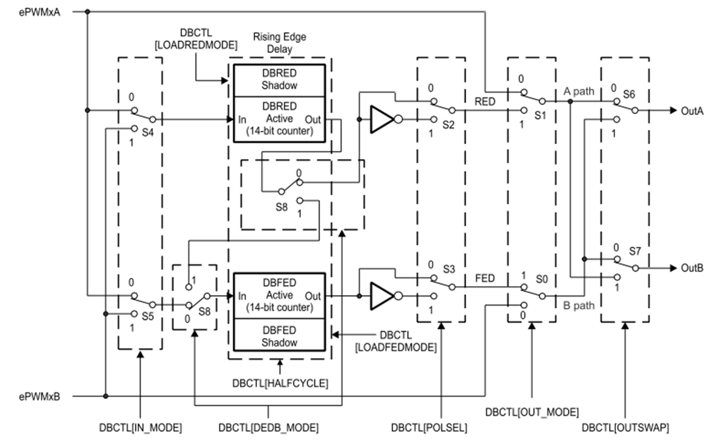
Fortunately, with the DBCTL[OUT_MODE] register in the dead-band submodule, as shown in Figure 2-3, it is possible to select the different sources for EPWMxB through a single bit change during the zero cross point. As shown in Figure 2-4, during the positive cycle, EPWM1B is sourced form EPWM1A together with both falling-edge and rising-edge delay enabled; during the negative cycle, EPWM1B bypasses the dead-band submodule and uses the original source with the normally high signal.
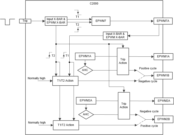
Finally, combined with the all the previous settings, the completed block diagram of the EPWM configurations can be found in Figure 2-5.
 Figure 2-3 Configuration Options for the
Dead-Band Submodule
 Figure 2-4 Different Sources Selection
for EPWM1B
 Figure 2-5 Block Diagram of the EPWM
Configurations
 The below codes, found in ISR1(), show the basic settings required during the zero-crossing point. The negative_flag and positive_flag are used to make sure the EPWM reconfiguration is implemented once.
    if(positive_cycle)
    {
        EPWM_setCounterCompareValue(S1_S3_PWM_BASE, EPWM_COUNTER_COMPARE_A,
                                    Test_Cmpa);
        if(negative_flag)
        {
            EPWM_setCounterCompareValue(S2_S4_PWM_BASE, EPWM_COUNTER_COMPARE_A,
                                        PERIOD_TICKS);
            EPWM_setDeadBandDelayMode(S1_S3_PWM_BASE, EPWM_DB_FED, true);
            EPWM_setDeadBandDelayMode(S2_S4_PWM_BASE, EPWM_DB_FED, false);

            EPWM_setTripZoneAction(S1_S3_PWM_BASE, EPWM_TZ_ACTION_EVENT_TZB,
                                 EPWM_TZ_ACTION_LOW);
            EPWM_setTripZoneAction(S2_S4_PWM_BASE, EPWM_TZ_ACTION_EVENT_TZB,
                                 EPWM_TZ_ACTION_DISABLE);

            negative_flag=0;
            positive_flag=1;
        }
    }

    else
    {
        EPWM_setCounterCompareValue(S2_S4_PWM_BASE, EPWM_COUNTER_COMPARE_A,
                                    Test_Cmpa);
        if(positive_flag)
        {
            EPWM_setCounterCompareValue(S1_S3_PWM_BASE, EPWM_COUNTER_COMPARE_A,
                                        PERIOD_TICKS);
            EPWM_setDeadBandDelayMode(S1_S3_PWM_BASE, EPWM_DB_FED, false);
            EPWM_setDeadBandDelayMode(S2_S4_PWM_BASE, EPWM_DB_FED, true);

            EPWM_setTripZoneAction(S1_S3_PWM_BASE, EPWM_TZ_ACTION_EVENT_TZB,
                                   EPWM_TZ_ACTION_DISABLE );
            EPWM_setTripZoneAction(S2_S4_PWM_BASE, EPWM_TZ_ACTION_EVENT_TZB,
                                   EPWM_TZ_ACTION_LOW);

            positive_flag =0;
            negative_flag = 1;
        }
    }
Table 2-1 has also summarized the different EPWM settings for positive and negative cycles. During the zero crossing point, CBC protection and normal operation actions should be swapped for EPWM1 and EPWM2. For example, at the transition from negative cycle to positive cycle, EPWM1B should change to be complementary to EPWM1A, by enabling the dead-band mode for EPWM1B, while EPWM2B needs to bypass the dead-band mode. Beside, CBC trip action should be disabled for EPWM2B and enabled for EPWM1B, so that EPWM2B state will be only influenced by T1 and T2 events to achieve delayed protection. Also, the switching for Test_Cmpa ↔ PERIOD_TICKS for the CMPA register should be taken care, where CMPA is directly related to the duty cycle provided by the control loop, that is CMPA=(1- duty cycle)* PERIOD_TICKS.
| PWM Signals | Basic Settings | Positive Cycle | Negative Cycle |
|---|---|---|---|
| EPWM1A-S1 | ↑ CAU, PRD ↓ ZRO, CAD Enable CBC, forced low action |
CMPA = Test_Cmpa | CMPA = PERIOD_TICKS |
| EPWM2B-S2 | One time Software Force high; active high complementary to
EPWM2A; ↓T1 ↑T2 T1 = DCBEVT1(EPWM7A high) T2 = DCBEVT2(EPWM7A low) Enable CBC |
Bypass dead-band mode; Disable CBC action |
Enable dead-band mode;Enable CBC forced low action |
| EPWM1B-S3 | One time Software Force high;active high complementary to
EPWM1A; ↓T1 ↑T2 T1 = DCBEVT1(EPWM7A high) T2 = DCBEVT2(EPWM7A low) Enable CBC |
Enable dead-band mode; Enable CBC forced low action |
Bypass dead-band mode; Disable CBC trip action |
| EPWM2A-S4 | ↑ CAU, PRD ↓ ZRO, CAD |
CMPA = PERIOD_TICKS | CMPA = Test_Cmpa |
| EPWM7A | ↑ T1 ↓ T2 RED = trip_delay (1us), T1 = DCBEVT1(Trip low), T2 = DCBEVT2(Trip high ) |
||