SPRACZ1 October 2021 F29H850TU , F29H859TU-Q1 , TMS320F280021 , TMS320F280021-Q1 , TMS320F280023 , TMS320F280023-Q1 , TMS320F280023C , TMS320F280025 , TMS320F280025-Q1 , TMS320F280025C , TMS320F280025C-Q1 , TMS320F280040-Q1 , TMS320F280040C-Q1 , TMS320F280041 , TMS320F280041-Q1 , TMS320F280041C , TMS320F280041C-Q1 , TMS320F280045 , TMS320F280048-Q1 , TMS320F280048C-Q1 , TMS320F280049 , TMS320F280049-Q1 , TMS320F280049C , TMS320F280049C-Q1 , TMS320F28044 , TMS320F28075 , TMS320F28075-Q1 , TMS320F28076 , TMS320F28374D , TMS320F28374S , TMS320F28375D , TMS320F28375S , TMS320F28375S-Q1 , TMS320F28376D , TMS320F28376S , TMS320F28377D , TMS320F28377D-EP , TMS320F28377D-Q1 , TMS320F28377S , TMS320F28377S-Q1 , TMS320F28378D , TMS320F28378S , TMS320F28379D , TMS320F28379D-Q1 , TMS320F28379S , TMS320F28384D , TMS320F28384D-Q1 , TMS320F28384S , TMS320F28384S-Q1 , TMS320F28386D , TMS320F28386D-Q1 , TMS320F28386S , TMS320F28386S-Q1 , TMS320F28388D , TMS320F28388S , TMS320F28P650DH , TMS320F28P650DK , TMS320F28P650SH , TMS320F28P650SK , TMS320F28P659DH-Q1 , TMS320F28P659DK-Q1 , TMS320F28P659SH-Q1
3 Test Results
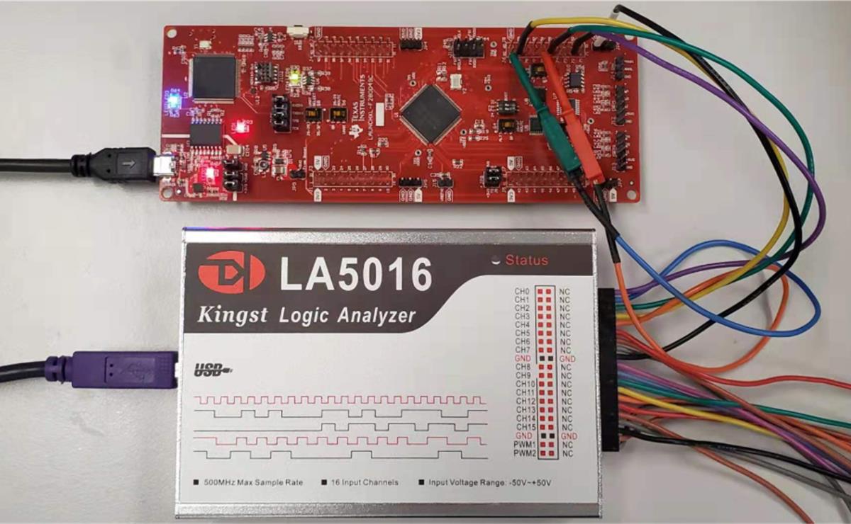
The delayed protection scheme has been validated with the LaunchPad LAUNCHXL-F280049C. In the given example codes, changing positive_cycle to 1 or 0 to decide positive cycle or negative cycle operation; changing simulate_EPWM_Cmpa value to provide different time scale for the trip signal (EPWM8A). The test results are measured with the Kingst Logic Analyzer, as shown in Figure 3-1.
 Figure 3-1 Test platform Setup
Figure 3-2 shows the condition of trip signal during positive cycle, where EPWM1A starts CBC protection right at the trip low event, while EPWM2B turns low after a delay of 1.12 µs measured. Since EPWM2B needs to follow the action of EPWM7A, the actual delay would be a bit longer than the defined value of 1 µs. Figure 3-3 shows the trip signal during negative cycle, where the delayed protection logic also works as expected.
 Figure 3-2 Trip Signal during Positive
Cycle
 Figure 3-3 Trip Signal during Negative
Cycle