SPRAD13 May 2022 AM623 , AM625
- Abstract
- Trademarks
- 1 Introduction
- 2 Via Channel Arrays
- 3 Width/Spacing Proposal for Escapes
- 4 Stackup
- 5 Via Sharing
- 6 Floorplan Component Placement
- 7 Critical Interfaces Impact Placement
- 8 Routing Priority
- 9 SerDes Interfaces
- 10DDR Interfaces
- 11Power Decoupling
- 12Route Lowest Priority Interfaces Last
- 13Summary
9 SerDes Interfaces
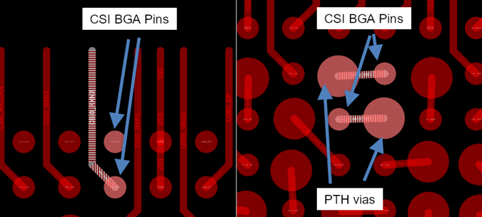
The package BGA ball map is also arranged to support routing the highest priority interfaces first. Therefore, the SerDes CSI interfaces are located on the outer two rings. The differential receive pair should be routed away from the SoC on the top layer leaving a gap without blocking vias. The lanes located on inner BGA rows will require vias to escape as a differential pair on the bottom or on an interior layer. The VCA facilitates this for inner rows. See Figure 9-1 for an example of the escape of the SerDes signals on the AM62 board on the top layer and on an inner layer. Wide traces can limit the signal loss but could violate the impedance requirements. For more detailed information on routing Serdes signals refer to the document on High-Speed Interface Layout Guidelines. An example of the routing of CSI signals between the AM62 SoC and a connector on the AM62 SK EVM board is shown in Figure 9-2.
 Figure 9-1 Serdes CSI Escapes for TOP layer (Left) and Inner layer (Right)
 Figure 9-2 CSI 2-Lane Routing