SPRAD64 November 2022 AM620-Q1 , AM623 , AM625 , AM625-Q1
9 DDR Interfaces
The AM62x (AMC) supports connection to either a DDR4 or LPDDR4 device. The DDR signals must be routed next. Refer to the DDR Routing Guidelines document for detailed recommendations for DDR routing. The images below show the BGA breakout for the DDR interface on the AM62x (AMC) Board. Routing for both DDR4 and LPDDR4 use a similar escape, with LPDDR4 requiring a lesser number of signals.
The DDR SDRAM memory devices are normally arranged so that the data group balls are closest to the AM62x (AMC) device. The Package BGA ball map has been planned to place the DDR address and command signals between data byte lane 1 and data byte lane0.
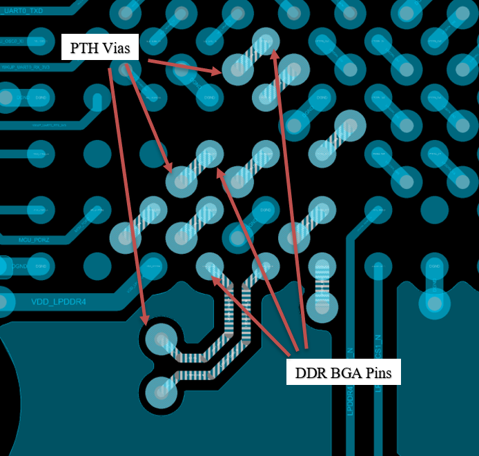
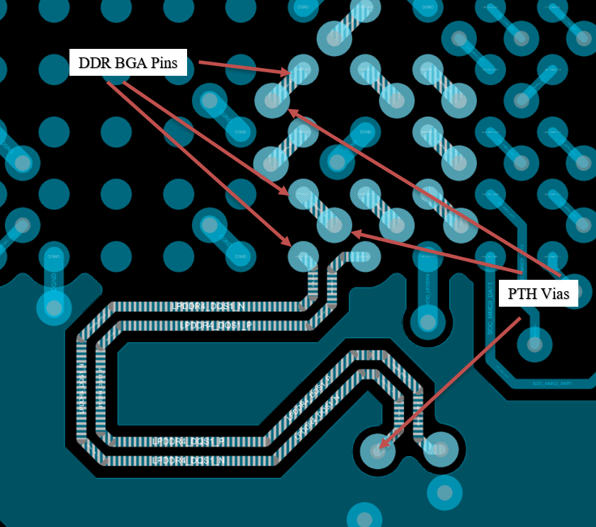
Figure 9-1 and Figure 9-2 illustrate how to escape the DDR byte lanes 0 and 1, respectively. The use of Plated Through Hole (PTH) vias make the routing of these signals between the SoC and SDRAM possible on any layer.
 Figure 9-1 DDR Byte Lane0 Escape
 Figure 9-2 DDR Byte Lane1 Escape
The address, command, and clock signals are routed directly to the memory device.
The top and inner layers are used to escape and route the address and command signals. The traces must be length matched to ensure that the signals arrive at the memory at the same time. Length matching must be from the SoC to memory pin individually and must include the stub to the memory pad and all via lengths. Refer to the DDR Routing Guidelines document for detailed recommendations for DDR routing.
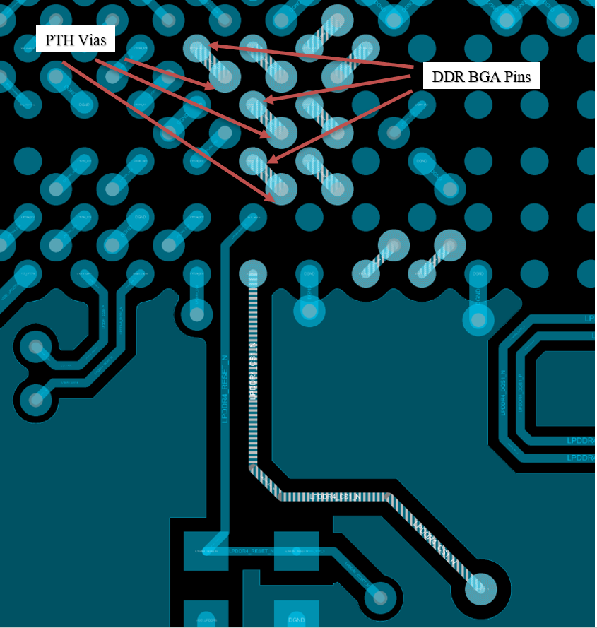
 Figure 9-3 DDR Address/Cmd Escape
The escapes of the address and command signals on these layers are shown above in Figure 9-3.
Address signals were routed directly from the SoC to the via next to the associated pad for the memory device. This requires that the address signals escape in the correct order. It is required to have the same number of vias for each of the address and command signals. The use of Plated Through Hole (PTH) vias allows the flexibility of routing the address/cmd signals on any layer.