SPRUI78D March 2019 – January 2022 TMS320F28075 , TMS320F28075-Q1 , TMS320F28076 , TMS320F28374D , TMS320F28374S , TMS320F28375D , TMS320F28375S , TMS320F28375S-Q1 , TMS320F28376D , TMS320F28376S , TMS320F28377D , TMS320F28377D-Q1 , TMS320F28377S , TMS320F28377S-Q1 , TMS320F28378D , TMS320F28378S , TMS320F28379D , TMS320F28379D-Q1 , TMS320F28379S
- Trademarks
- 1 Introduction
- 2 System Integrator Development Interface Agreement
- 3 C2000 Development Process for Management of Systematic Faults
- 4 TMS320F2837xD/S and TMS320F2807x MCU Architecture for Management of Random Faults
- 5 Brief Description of Safety Elements
-
6 Brief Description of Diagnostics
- 6.1
C2000 MCU Infrastructure Components
- 6.1.1 Clock Integrity Check Using CPU Timer
- 6.1.2 Clock Integrity Check Using HRPWM
- 6.1.3 EALLOW and MEALLOW Protection for Critical Registers
- 6.1.4 Efuse Autoload Self-Test
- 6.1.5 Efuse ECC
- 6.1.6 Efuse ECC Logic Self-Test
- 6.1.7 External Clock Monitoring via XCLKOUT
- 6.1.8 External Monitoring of Warm Reset (XRSn)
- 6.1.9 External Voltage Supervisor
- 6.1.10 External Watchdog
- 6.1.11 Glitch Filtering on Reset Pins
- 6.1.12 Hardware Disable of JTAG Port
- 6.1.13 Internal Watchdog (WD)
- 6.1.14 Lock Mechanism for Control Registers
- 6.1.15 Missing Clock Detect (MCD)
- 6.1.16 NMIWD Reset Functionality
- 6.1.17 NMIWD Shadow Registers
- 6.1.18 Multi-Bit Enable Keys for Control Registers
- 6.1.19 Online Monitoring of Temperature
- 6.1.20 Periodic Software Read Back of Static Configuration Registers
- 6.1.21 Peripheral Clock Gating (PCLKCR)
- 6.1.22 Peripheral Soft Reset (SOFTPRES)
- 6.1.23 PLL Lock Profiling Using On-Chip Timer
- 6.1.24 Reset Cause Information
- 6.1.25 Software Read Back of Written Configuration
- 6.1.26 Software Test of ERRORSTS Functionality
- 6.1.27 Software Test of Missing Clock Detect Functionality
- 6.1.28 Software Test of Reset
- 6.1.29 Software Test of Watchdog(WD) Operation
- 6.2
Processing Elements
- 6.2.1 CLA Handling of Illegal Operation and Illegal Results
- 6.2.2 CLA Liveness Check Using CPU
- 6.2.3 CPU Hardware Built-In Self-Test (HWBIST)
- 6.2.4 CPU Hardware Built-In Self-Test (HWBIST) Auto-Coverage
- 6.2.5 CPU Hardware Built-In Self-Test (HWBIST) Fault Injection Capability
- 6.2.6 CPU Hardware Built-In Self-Test (HWBIST) Timeout Feature
- 6.2.7 CPU Handling of Illegal Operation, Illegal Results and Instruction Trapping
- 6.2.8 Reciprocal Comparison by Software
- 6.2.9 Software Test of CLA
- 6.2.10 Stack Overflow Detection
- 6.2.11 VCU CRC Check of Static Memory Contents
- 6.2.12 VCU CRC Auto Coverage
- 6.2.13 Disabling of Unused CLA Task Trigger Sources
- 6.3
Memory (Flash, SRAM and ROM)
- 6.3.1 Bit Multiplexing in Flash Memory Array
- 6.3.2 Bit Multiplexing in SRAM Memory Array
- 6.3.3 Data Scrubbing to Detect/Correct Memory Errors
- 6.3.4 Flash ECC
- 6.3.5 Flash Program Verify and Erase Verify Check
- 6.3.6 Software Test of ECC Logic
- 6.3.7 Software Test of Flash Prefetch, Data Cache and Wait-States
- 6.3.8 Access Protection Mechanism for Memories
- 6.3.9 SRAM ECC
- 6.3.10 SRAM Parity
- 6.3.11 Software Test of Parity Logic
- 6.3.12 Software Test of SRAM
- 6.4
On-Chip Communication Including Bus-Arbitration
- 6.4.1 1oo2 Software Voting Using Secondary Free Running Counter
- 6.4.2 DMA Overflow Interrupt
- 6.4.3 Event Timestamping Using IPC Counter
- 6.4.4 Maintaining Interrupt Handler for Unused Interrupts
- 6.4.5 Majority Voting and Error Detection of Link Pointer
- 6.4.6 PIE Double SRAM Comparison Check
- 6.4.7 PIE Double SRAM Hardware Comparison
- 6.4.8 Power-Up Pre-Operational Security Checks
- 6.4.9 Software Check of X-BAR Flag
- 6.4.10 Software Test of ePIE Operation Including Error Tests
- 6.4.11 Disabling of Unused DMA Trigger Sources
- 6.4.12 IPC 64-Bit Counter Value Plausibility Check
- 6.5
Digital I/O
- 6.5.1 ECAP Application Level Safety Mechanism
- 6.5.2 ePWM Application Level Safety Mechanism
- 6.5.3 ePWM Fault Detection Using XBAR
- 6.5.4 ePWM Synchronization Check
- 6.5.5 eQEP Application Level Safety Mechanisms
- 6.5.6 eQEP Quadrature Watchdog
- 6.5.7 eQEP Software Test of Quadrature Watchdog Functionality
- 6.5.8 Hardware Redundancy
- 6.5.9 HRPWM Built-In Self-Check and Diagnostic Capabilities
- 6.5.10 Information Redundancy Techniques
- 6.5.11 Monitoring of ePWM by eCAP
- 6.5.12 Monitoring of ePWM by ADC
- 6.5.13 Online Monitoring of Interrupts and Events
- 6.5.14 SDFM Comparator Filter for Online Monitoring
- 6.5.15 SD Modulator Clock Fail Detection Mechanism
- 6.5.16 Software Test of Function Including Error Tests
- 6.6
Analogue I/O
- 6.6.1 ADC Information Redundancy Techniques
- 6.6.2 ADC Input Signal Integrity Check
- 6.6.3 ADC Signal Quality Check by Varying Acquisition Window
- 6.6.4 CMPSS Ramp Generator Functionality Check
- 6.6.5 DAC to ADC Loopback Check
- 6.6.6 DAC to Comparator Loopback Check
- 6.6.7 Opens/Shorts Detection Circuit for ADC
- 6.6.8 VDAC Conversion by ADC
- 6.6.9 Disabling Unused Sources of SOC Inputs to ADC
- 6.7
Data Transmission
- 6.7.1 Bit Error Detection
- 6.7.2 CRC in Message
- 6.7.3 DCAN Acknowledge Error Detection
- 6.7.4 DCAN Form Error Detection
- 6.7.5 DCAN Stuff Error Detection
- 6.7.6 EMIF Access Latency Profiling Using On-Chip Timer
- 6.7.7 EMIF Access Protection Mechanism
- 6.7.8 EMIF Asynchronous Memory Timeout Protection Mechanism
- 6.7.9 I2C Access Latency Profiling Using On-Chip Timer
- 6.7.10 Information Redundancy Techniques Including End-to-End Safeing
- 6.7.11 I2C Data Acknowledge Check
- 6.7.12 McBSP Receiver Overrun Detection
- 6.7.13 McBSP Receiver Sync Error Detection
- 6.7.14 McBSP Transmitter Sync Error Detection
- 6.7.15 McBSP Transmitter Underflow Detection
- 6.7.16 Parity in Message
- 6.7.17 SCI Break Error Detection
- 6.7.18 SCI Frame Error Detection
- 6.7.19 SCI Overrun Error Detection
- 6.7.20 Software Test of Function Using I/O Loopback
- 6.7.21 SPI Data Overrun Detection
- 6.7.22 Transmission Redundancy
- 6.1
C2000 MCU Infrastructure Components
- 7 Safety Architecture Configurations
- 8 Terms and Definitions
- 9 Summary of Safety Features and Diagnostics
- 10References
- 11Revision History
4.2.2 TMS320F2837xS and TMS320F2807x MCU Safety Philosophy
TMS320F2837xS and TMS320F2807x class of devices have a single CPU subsystem. The CPU subsystem has a pair of diverse processing units (C28x and CLA) with different hardware architecture, instruction set and software tools. Any of the two processing units can be used to execute main function (Level 1 of VDA E-gas concept).
The second processing unit of the CPU subsystem can be used for implementing Level 2 monitoring as illustrated in Figure 4-6. Due to diversity of the processing units, a 1oo1D architecture can be implemented using “reciprocal comparison by software in separate processing units” providing high diagnostic coverage for the processing units (ISO 26262-5, Table D.4 and IEC 61508-2, Table A.4). Heterogeneous CPU cores minimize possibility of common mode failures while implementing this reciprocal comparison thereby improving confidence in its Diagnostic Coverage. This implementation will have a single independent processing channel for TMS320F2837xS.
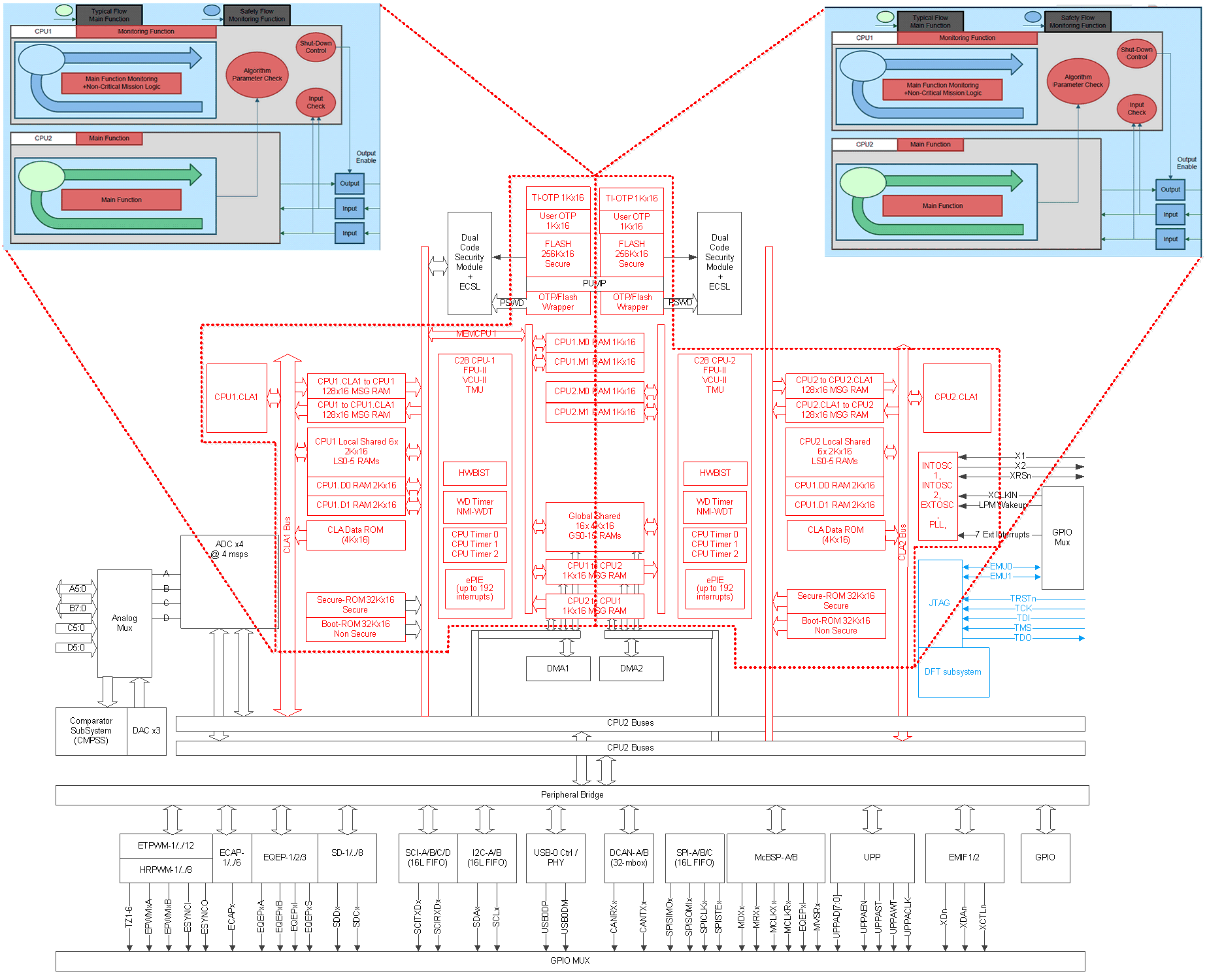
The product safety philosophy is explained based on 1oo1D safety configuration implemented using reciprocal comparison and other hardware diagnostics. Figure 4-8 illustrates safety partitioning based on the diagnostics employed. The various layers implemented are:
- Reciprocal Comparison Layer (RED) – This is the region of logic used for all processing operations. This logic has a one processing unit executing the main functionality (Level 1), second processing unit with specific assumptions of use and other hardware diagnostic elements executing monitoring functionality (Level 2). The memories closely coupled with C28x and CLA are protected with either ECC or parity. This region with high diagnostic coverage for both single point faults and latent faults can be used for performing software diagnostic on other design elements. The diverse processing (C28x and CLA) have different hardware architecture, instruction set and software tools. However, they share common power, clock, reset, bus and infrastructure elements. System integrator needs to independently perform common cause failure analysis and freedom from interference analysis and implement the necessary safety measures (for example, External Watchdog, Access Protection Mechanism for Memories, and so forth) to address the concerns which may come up from the analysis.
- Blended Layer (BLACK) – This is the region of logic that includes safety critical peripherals. This region has a mix of (predominantly) software and hardware diagnostics. Application protocols (for example, end-to-end Safeing techniques used in communication protocols) and application related checks (for example, measured values falls within the safe operating limit) are used to support functionally safe operation.
- Offline Layer (BLUE) – This region of logic has very limited or no integrated hardware diagnostics. Many features in this layer (for example, debug, test, calibration functions, and so forth) are used for production test or application debug and not used during regular operation. Techniques are employed to avoid freedom from interference to main application by the logic elements in this layer.
Due to the inherent versatility of the device architecture, several software voting based safety configurations are possible. Some of the safety configurations possible with TMS320F2837xD for improving diagnostic coverage are explained in Table 7-1. While implementing these configurations, system integrator needs to consider the potential common mode failures and address them in an appropriate manner. This may suitably be modified to adapt to TMS320F2837xS and TMS320F2807x requirements based on the availability of processing units. (As stated earlier, the device claims no hardware fault tolerance, (for example, no claims of HFT > 0), as defined in IEC 61508:2010).
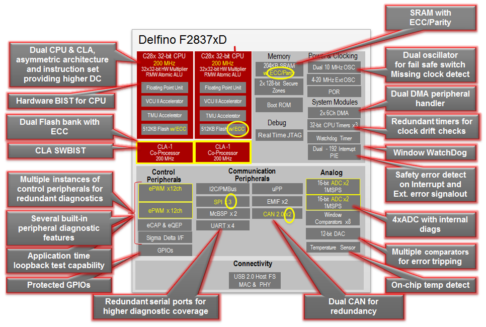
 Figure 4-7 C2000 MCU
Delfino F2837xD With Safety Features
 Figure 4-8 C2000 MCU
Delfino F2837xD Device Block Diagram With Safety Partitioning