SPRUIF3B May 2017 – March 2019 DRA790 , DRA791 , DRA793 , DRA797
-
DRA79x EVM CPU board
- Trademarks
- 1 Introduction
- 2 Overview
- 3
Hardware
- 3.1 Hardware Architecture
- 3.2 DRA71x, DRA79x, TDA2E-17, and AM570x Processor
- 3.3 Power Architecture
- 3.4 Reset Structure
- 3.5 Clocks
- 3.6
Memory
- 3.6.1 SDRAM Memory
- 3.6.2 QSPI Flash Memory
- 3.6.3 EMMC Flash Memory
- 3.6.4 MicroSD Card Cage
- 3.6.5 GPMC NOR Flash Memory
- 3.6.6 GPMC NAND Flash Memory
- 3.6.7 Boot Modes
- 3.6.8 JTAG/Emulator and Trace
- 3.6.9 UART Terminal
- 3.6.10 DCAN and CAN Interfaces
- 3.6.11 Universal Serial Bus (USB)
- 3.6.12 Wired Ethernet
- 3.6.13 Video Output
- 3.6.14 Video Input
- 3.6.15 Mini-PCIe
- 3.6.16 Media Local Bus (MLB)
- 3.6.17 Audio
- 3.6.18 COM8 Module Interface
- 3.6.19 eFuse Programming Supply
- 3.6.20 User Interface LEDs
- 3.6.21 Power Monitoring
- 3.6.22 I2C Peripheral Map
- 3.6.23 GPIO List
- 3.6.24 I/O Expander List
- 3.6.25 Configuration EEPROM
- 4
Signal Multiplex Logic
- 4.1 GPMC and QSPI Selection (MUX A)
- 4.2 GPMC, VIN1, and VOUT3 Selection (MUX B)
- 4.3 GPMC and EMMC Selection (MUX C)
- 4.4 VIN2A and EMU Selection (MUX D, MUX E)
- 4.5 VIN2A and RGMII1 Selection (MUX F)
- 4.6 RGMII0 and VIN1B Selection (MUX J)
- 4.7 SPI2 and UART3 Selection (MUX K)
- 4.8 DCAN2 and I2C3 Selection (MUX L)
- 5 USB3 Supported Configurations
- 6 References
- Revision History
3.4 Reset Structure
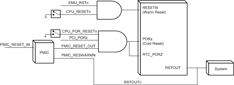
Figure 7 shows the reset structure. The power-on reset timing is primarily controlled from the system power ICs (LP8733 and LP8732). Two push-buttons are provided for user-controlled resets. One button is the power on reset (SW4) for a complete SoC reset. The other button is for a warm reset (SW5). The warm reset can also be sourced from the MIPI-60 JTAG/Trace connector.
 Figure 7. Reset Structure
 Table 5 summarizes the reset signals.
Table 5. Reset Signals Structure
| Reset Type | Reset Signal Sources | Comments |
|---|---|---|
| Power-On Reset (PORn)
(as whole system reset) |
CPU_POR_RESETn | PORn reset push-button |
| PCI_PORz | PCIe inbound reset | |
| PMIC_RESET_OUT | Power on reset from power ICs | |
| Warm Reset | CPU_RESETn | Warm reset push-button |
| EMU_RSTn | Reset from Emulator | |
| PMIC Power-On Reset | PMIC_RESET_IN | PMIC reset input |
| Processor Reset Out | RSTOUTn | Reset output from processor to system, PMIC (warm reset input) |