SPRUIM6A October 2018 – November 2020
- 1Introduction
- 2AM65x IDK Overview
-
3Common Processor Board
- 3.1 Key Features
- 3.2 Functional Block Diagram
- 3.3
Overview of Common Processor Board
- 3.3.1 Clocking
- 3.3.2 Reset
- 3.3.3 Power Requirements
- 3.3.4 Configuration
- 3.3.5 Memory Interfaces
- 3.3.6 Ethernet Interface
- 3.3.7 LCD Display Interface
- 3.3.8 USB 2.0 Interface
- 3.3.9 CSI-2 Interface
- 3.3.10 Application Card Interface
- 3.3.11 SERDES Interface
- 3.3.12 GPMC/DSS Interface
- 3.3.13 I2C Interface
- 3.3.14 SPI Interface
- 3.3.15 Timer and Interrupt
- 3.3.16 Fan Connector
- 4IDK Application Card
- 5x2 Lane PCIe Personality Card
-
6Known Issues
- 6.1 Determining the Revision and Date Code for the EVM
- 6.2 Known Issues for the A, E4, and E3 Revision
- 6.3 Known Issues for the E4 & E3 Revision
- 6.4
Known Issues for the E3 Revision
- 6.4.1 Resonance Observed on the SoC Side of Some Filters Associated with VDDA_1V8
- 6.4.2 Additional LDO Power Supply Needed for VDDA_1P8_SERDES0
- 6.4.3 Length of the RESET Signal to the PCIE Connectors on the SERDES Daughter Card
- 6.4.4 The PORz_OUT and MCU_PORz_OUT Signals Go High During Power Sequencing
- 6.4.5 Orientation of the Current Monitoring Shunt Resistors
- 6.4.6 SD Card IO Supply Capacitance
- 6.4.7 PHY Resistor Strapping Changed to Disable EEE Mode
- 6.4.8 The I2C Address for the I2C Boot Memory changed to 0x52
- 7Configuring the PRG0 and PRG1 Ethernet Interface to MII
- 8Revision History
3.3.14 SPI Interface
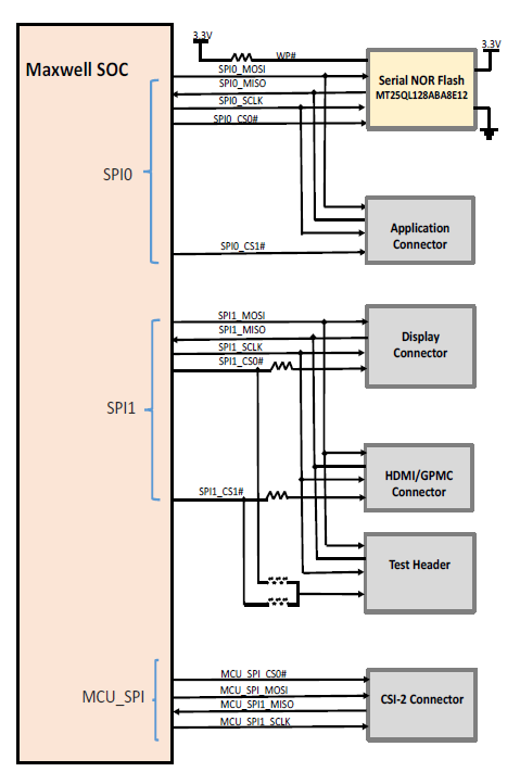
Of the six SPI interfaces supported by the AM65x processor, three are used on the processor card:
- SPI0: A 128-Mbit SPI NOR Flash of part number MT25QL128ABA8E12 is interfaced to the SPI0 port of the AM65x. In addition, SPI0 is also connected to the application connector. SPI_CS0 and SPI_CS1 chip select signals are used for the serial flash and application connector, respectively.
- SPI1 is connected to the display connector, GPMC/DSS connector, and test header. The SPI1 interface signals are at a 3.3-V I/O level. SPI1_CS0 is connected to the display connector and SPI_CS1 is connected to the GPMC/DSS connector. The chip selects SPI1_CS0 and SPI_CS1 are also connected to the test header, through resistors (R316 and R317) as shown in Table 3-35. By default, these resistors are not installed. To use the SPI functionality on the header, either R316 or R317 must be mounted. Pin-outs of the test header (J20) are given in Table 3-34.
Table 3-34 SPI1 Header (J20) Pin-out
Pin no. Signal 1 SPI1_MOSI 2 SPI1_MISO 3 SPI1_CS 4 SPI1_CLK 5 DGND Table 3-35 Resistors for Selecting CS Signals for Test Automation HeaderSelected SPI1_CS Signal for Test Header Mount Unmount SPI1_CS1 R316 R311 SPI1_CS0 R317 R675 - The MCU_SPI is interfaced to the CSI-2 connector.
The SPI0 and SPI1 interface signals are powered by the VDDSHV_GENERAL power supply of SoC and are at the 3.3-V I/O level.
The MCU_SPI interface signals are powered by the VDDSHV_WKUP_GENERAL power supply of SoC and are at the 3.3-V I/O level.
 Figure 3-24 SPI Tree