SPRUIW3 October 2021 TMS320F280033 , TMS320F280034 , TMS320F280034-Q1 , TMS320F280036-Q1 , TMS320F280036C-Q1 , TMS320F280037 , TMS320F280037-Q1 , TMS320F280037C , TMS320F280037C-Q1 , TMS320F280038-Q1 , TMS320F280038C-Q1 , TMS320F280039 , TMS320F280039-Q1 , TMS320F280039C , TMS320F280039C-Q1 , TMS320F280040-Q1 , TMS320F280040C-Q1 , TMS320F280041 , TMS320F280041-Q1 , TMS320F280041C , TMS320F280041C-Q1 , TMS320F280045 , TMS320F280048-Q1 , TMS320F280048C-Q1 , TMS320F280049 , TMS320F280049-Q1 , TMS320F280049C , TMS320F280049C-Q1
- Trademarks
- 1Feature Differences Between F28004x and F28003x
- 2PCB Hardware Changes
-
3Feature Differences for System Consideration
- 3.1
New Features in F28003x
- 3.1.1 TMU Type1
- 3.1.2 Fast Integer Division (FINTDIV)
- 3.1.3 Host Interface Controller (HIC)
- 3.1.4 Background CRC (BGCRC)
- 3.1.5 Standby Low Power Mode
- 3.1.6 X1 GPIO Functionality
- 3.1.7 Diagnostic Features (PBIST/HWBIST)
- 3.1.8 Advance Encryption Standard (AES)
- 3.1.9 Secure Boot/JTAG Lock
- 3.1.10 Modular Controller Area Network (MCAN)
- 3.1.11 Embedded Pattern Generator (EPG)
- 3.1.12 Live Firmware Update (LFU)
- 3.2 Communication Module Changes
- 3.3 Control Module Changes
- 3.4 Analog Module Differences
- 3.5 Other Device Changes
- 3.6 Power Management
- 3.7 Memory Module Changes
- 3.8 GPIO Multiplexing Changes
- 3.9 Analog Multiplexing Changes
- 3.1
New Features in F28003x
- 4Application Code Migration From F28004x to F28003x
- 5Specific Use Cases Related to F28003x New Features
- 6EABI Support
- 7References
2.1.2 100-Pin PZ Migration for New PCB Design
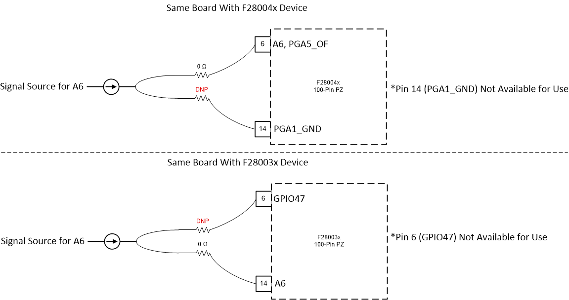
If the PCB is yet to be designed and you are moving from F28004x/F28003x to F28003x/F28004x, respectively, the dual routing technique illustrated in Figure 2-2 maximizes pin utilization. The complete pin migration is outlined in Table 2-2.
 Figure 2-2 Dual Routing Technique
Illustrated
Figure 2-2 Dual Routing Technique
IllustratedFor the color legend, see Figure 2-1.
| Pin No | Pin Name | Transition Type | Action | ||
|---|---|---|---|---|---|
| F28004x | F28003x | F28003x to F28004x | F28004x to F28003x | ||
| Minor Incompatibility - Signals in Common (1) | |||||
| 28 | PGA6_IN, C5 | C5, A12 | Common Analog Channel | Use C5 | |
| 31 | PGA4_IN, C3 | C3, A7 | Use C3 | ||
| 36 | A4, B8, PGA2_OF | A4, B8 | Use A4 or B8 | ||
| 37 | A8, PGA6_OF | A8 | Use A8 | ||
| 39 | B4, C8, PGA4_OF | B4, C8 | Use B4 or C8 | ||
| 40 | A10, B1, C10, PGA7_OF | A10, B1, C10 | Use A10, B1 or C10 | ||
| 21 | C2 | C2, B12 | Use C2 | ||
| 22 | A1, DACB_OUT | A1, DACB_OUT, B7 | Use A1 or DACB_OUT | ||
| 41 | B0 | B0, C11 | Use B0 | ||
| 69 | X1 | GPIO19, X1 | Common Clock | GPIO19 not available for use | |
| 81 | GPIO23_VSW | GPIO23 | Common GPIO | Do not use DCDC. GPIO22 & GPIO23 available for use | |
| 83 | GPIO22_VFBSW | GPIO22 | |||
| Medium Incompatibility - Different Signals, Same Type | |||||
| 19 | C0 | A14, B14, C4 | Analog Function Compatible | Update code to C0 | Update code to A14, B14 or C4 |
| 85 | GPIO40 | GPIO44 | GPIO Function Compatible | Update code to GPIO40 | Update code to GPIO44 |
| 91 | GPIO39 | GPIO61 | Update code to GPIO39 | Update code to GPIO61 | |
| Medium Incompatibility - Dual Routing | |||||
| 6 | A6, PGA5_OF | GPIO47 | Dual PCB Route, F28004x 0-Ohm Resistor, F28003x DNP | Dual route to Pin 6 & 14 | |
| 7 | B2, C6, PGA3_OF | GPIO48 | Dual route to Pin 7 & 15 | ||
| 8 | B3, VDAC | GPIO49 | Dual route to Pin 8 & 16 | ||
| 9 | A2, B6, PGA1_OF | GPIO50 | Dual route to Pin 9 & 17 | ||
| 10 | A3 | GPIO51 | Dual route to Pin 10 & 18 | ||
| 14 | PGA1_GND | A6 | Dual PCB Route, F28004x DNP, F28003x 0-Ohm Resistor | Dual route to Pin 6 & 14 | |
| 15 | PGA3_GND | B2, C6 | Dual route to Pin 7 & 15 | ||
| 16 | PGA5_IN | B3, VDAC | Dual route to Pin 8 & 16 | ||
| 17 | C4 | A2, B6, C9 | Dual route to Pin 9 & 17 | ||
| 18 | PGA1_IN | C7, B9, A3 | Dual route to Pin 10 & 18 | ||
| Major Incompatibility - Different Signals and Types | |||||
| 32 | PGA6_GND, PGA2_GND, PGA4_GND | B5 | PGA Ground to ADC Channel | Tie to VSS | |
| 42 | PGA7_GND | C14 | |||
| 13 | PGA5_GND | GPIO54 | PGA Ground to GPIO | Tie to VSS through 0-Ohm resistor. Depopulate resistor when using F28003x and enable internal pull-up for the GPIOs | |
| 12 | VSSA | GPIO53 | Ground to GPIO | ||
| 82 | VSS_SW | GPIO41 | |||
| 11 | VDDA | GPIO52 | Power to GPIO | Tie to VDDIO through 0-Ohm resistor. Depopulate resistor when using F28003x and enable internal pull-up for the GPIOs | |
| 80 | VDDIO_SW | GPIO40 | |||
| 20 | PGA3_IN | A11, B10, C0 | PGA Input to ADC Channel | No connect. Enable internal pull-up for the GPIOs on F28003x | |
| 30 | PGA2_IN | B11 | |||
| 43 | PGA7_IN | GPIO55 | PGA Input to GPIO | ||
| 44 | C14 | GPIO60 | Analog to GPIO | ||
| 48 | FLT2 | GPIO20, B5 | Flash Test Pins to GPIO | ||
| 49 | FLT1 | GPIO21, B11 | |||
- Channel to use selected in software.