SPRUJ06 October   2021


  1.   Trademarks
  2. 1Introduction
  3. 2Revisions and Assembly Variants
  4. 3System Description
    1. 3.1 Key Features
    2. 3.2 Functional Block Diagram
    3. 3.3 Interfaces and Major Component Description
      1. 3.3.1 Breakout Board Section
      2. 3.3.2 IO-Link Section Overview and Major Component Description
        1. 3.3.2.1 IO Link Transceiver TIOL111DMWR
        2. 3.3.2.2 Smart Switch TPS4H160BQPWPRQ1
        3. 3.3.2.3 Serializer SN65HVS882
        4. 3.3.2.4 INA253
        5. 3.3.2.5 LED Driver TLC59282
        6. 3.3.2.6 Signal Routing
      3. 3.3.3 Power Section
        1. 3.3.3.1 Power Input
      4. 3.3.4 Board Mating Connections
  5. 4Known Issues
    1. 4.1 Issue 1: Voltage Spike Across the TX Line of the Transceiver

Power Section

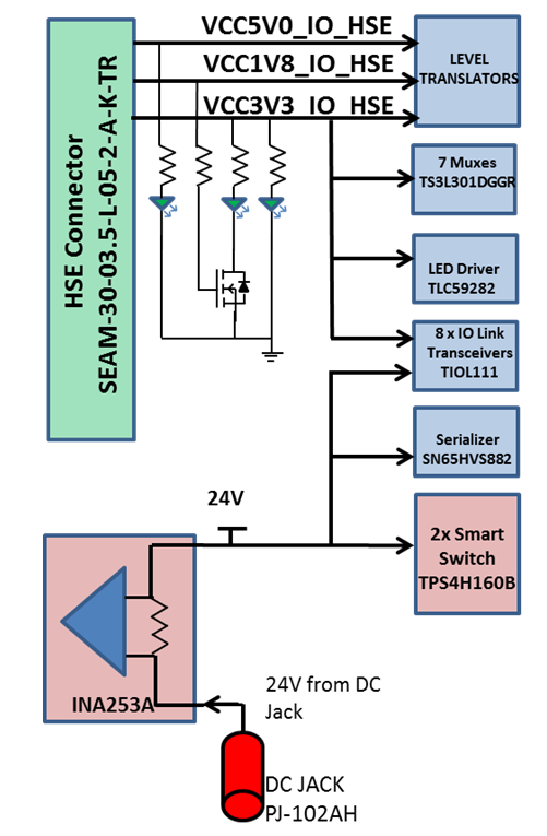
All necessary power required for the IO Link/Breakout Board are provided from the HSE connector and on board 24 V DC supply via DC jack. Power Good LED’s are provided for 5 V, 3.3 V and 1.8 V. Figure 3-5 shows the power section of the Breakout board.
GUID-A3EA0E98-F155-41D8-B903-F19005579C1C-low.png Figure 3-5 Power Input