SPRUJ15B November 2021 – October 2022
6 Hardware References
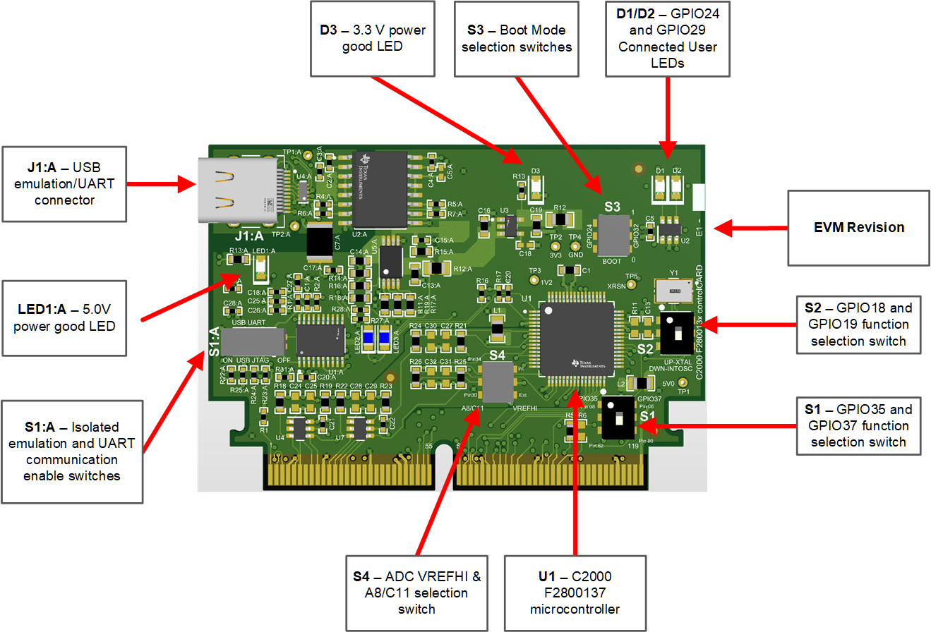
 Figure 6-1 Key Components on the
controlCARD - Front
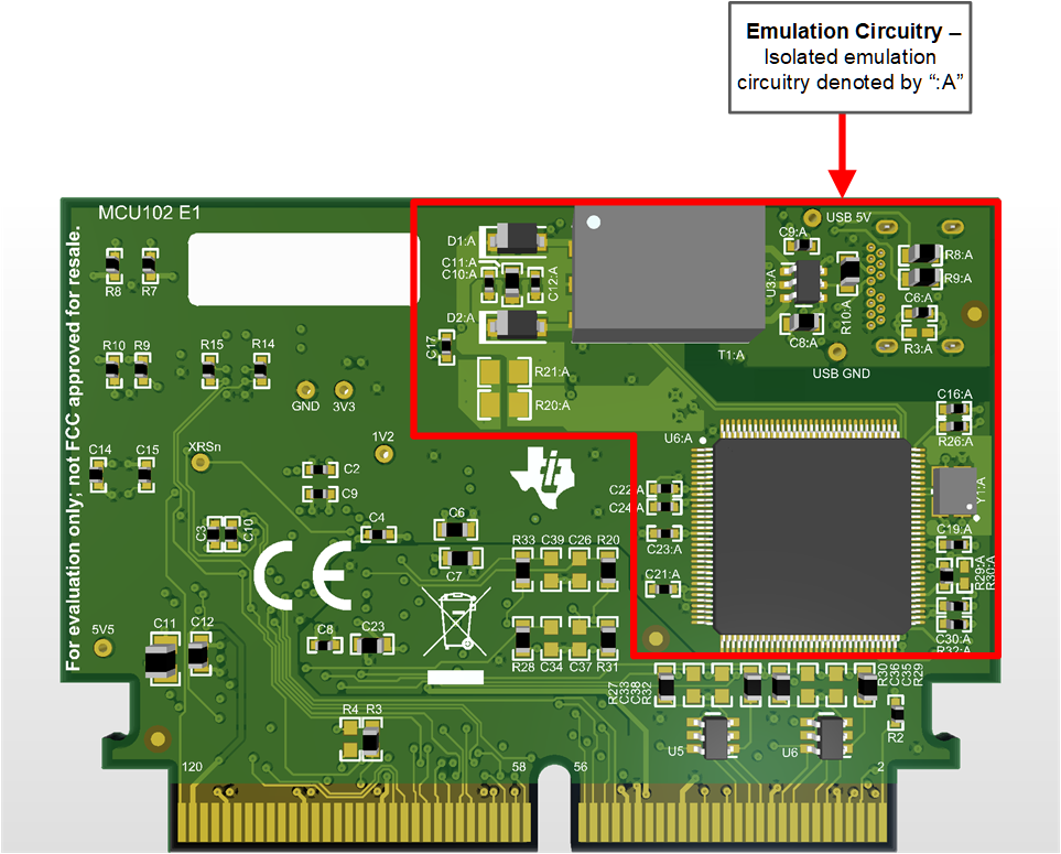
 Figure 6-2 Key Components on the
controlCARD - Back
| Connectors | |
|---|---|
| J1:A | Emulation/UART connector/Power - USB-C connector used to provide
XDS110 emulation and USB-to-UART (SCI) communication through MSP432
logic. S1:A determines which connections are enabled to the MCU. The USB-C connector also provides power on the controlCARD. |
| LEDs | |
|---|---|
| LED1:A | Turns on (red) when 5 V is supplied to the
controlCARD (5 V can be supplied either through the USB-C connector or externally through the HSEC connector) |
| LED2:A/LED3:A | JTAG/UART RX/TX toggle indicator (blue) |
| D1 | Controlled by GPIO–24 with negative logic (red) |
| D2 | Controlled by GPIO–39 with negative logic (red) |
| D3 | Turns on (green) when 3.3 V is supplied to the controlCARD from the on-board LDO (U3) |
| Resistors and Capacitors | |
|---|---|
| R18-R33 | ADC RC input filter resistors: Series resistors which can be used to create an RC filter on the ADC's input. |
| C24-C39 | ADC RC input filter capacitors: Optional capacitors, not populated by default, for the ADC input's RC filters. |
|
R11 and C13 |
External precision resistor. Optional external precision resistor (ExtR), no populated by default, to achieve better accuracy with INTOSC2. Refer to the F280013x data sheet for more information on the ExtR feature. |
| Switches | |
|---|---|
| S1:A | Isolated emulation and UART communication enable switches: |
S1:A
Position 1 – USB JTAG Enable:
|
|
S1:A
Position 2 – USB UART communication enable:
|
|
|
S1 |
GPIO35/TDI and GPIO37/TDO Function Switch: This switch selects the function of the GPIO35 and GPIO37 pins
|
| S2 | PWM6 or external crystal selection switch: This switch enables the use of PWM6 or an external crystal. This methodology was required to support the full range of TI's baseboards and is not recommended in a production system. For full details, see Section 5.2. |
| S3 | Boot Mode Switch: Controls the Boot Options of the F280013x device, see the Table 6-2. For a full description, see the device-specific data sheet. |
| S4 | Analog Configuration Switch: This switch selects the source for VREFHI and the routing of the A8/C11 ADC channel. |
S4
Position 1 (left switch) – ADC channel A8/C11 HSEC pin
selection
|
|
Position
2 (right switch) - ADC voltage reference selection.
Note that additional software configuration is required to enable the ADC internal or external voltage reference. |
|
| Test Points | |
|---|---|
| TP1:A | USB 5.0 V input: This is the 5 V supply from the USB-C connector. |
| TP2:A | USB GND input: This GND from the USB-C connector. |
| TP1 | HSEC 5.0 V input: 5.0 V input provided to the controlCARD. |
| TP2 | Unfiltered 3.3 V: Provides power to the F280013x device. |
| TP3 | MCU 1.2 V: VDD 'core supply' to the F280013x device. Note that this controlCARD has been designed to use the internal voltage regulator. |
| TP4 | Device Ground |
| TP5 | XRSn of F280013x device: Connected to the XRSn pin of the F280013x device. |
On the back of the controlCARD, test points are indicated by their signal.
| Mode | Switch Position 1 (left switch, GPIO-24) | Switch Position 2 (right switch, GPIO-32) | Boot From |
|---|---|---|---|
| 00 | 0 (down) | 0 (down) | Parallel I/O |
| 01 | 1 (up) | 0 (down) | SCI/Wait Boot |
| 02 | 0 (down) | 1 (up) | CAN |
| 03 | 1 (up) | 1 (up) | Flash/USB |