SPRUJE4A August 2024 – November 2024 F29H850TU , F29H859TU-Q1
- 1
- Description
- Get Started
- Features
- 5
- 1Evaluation Module Overview
- 2Hardware
- 3Software
- 4Hardware Design Files
- 5Additional Information
- 6References
- 7Revision History
2.1.1 Configuration 1: Stand-alone Configuration
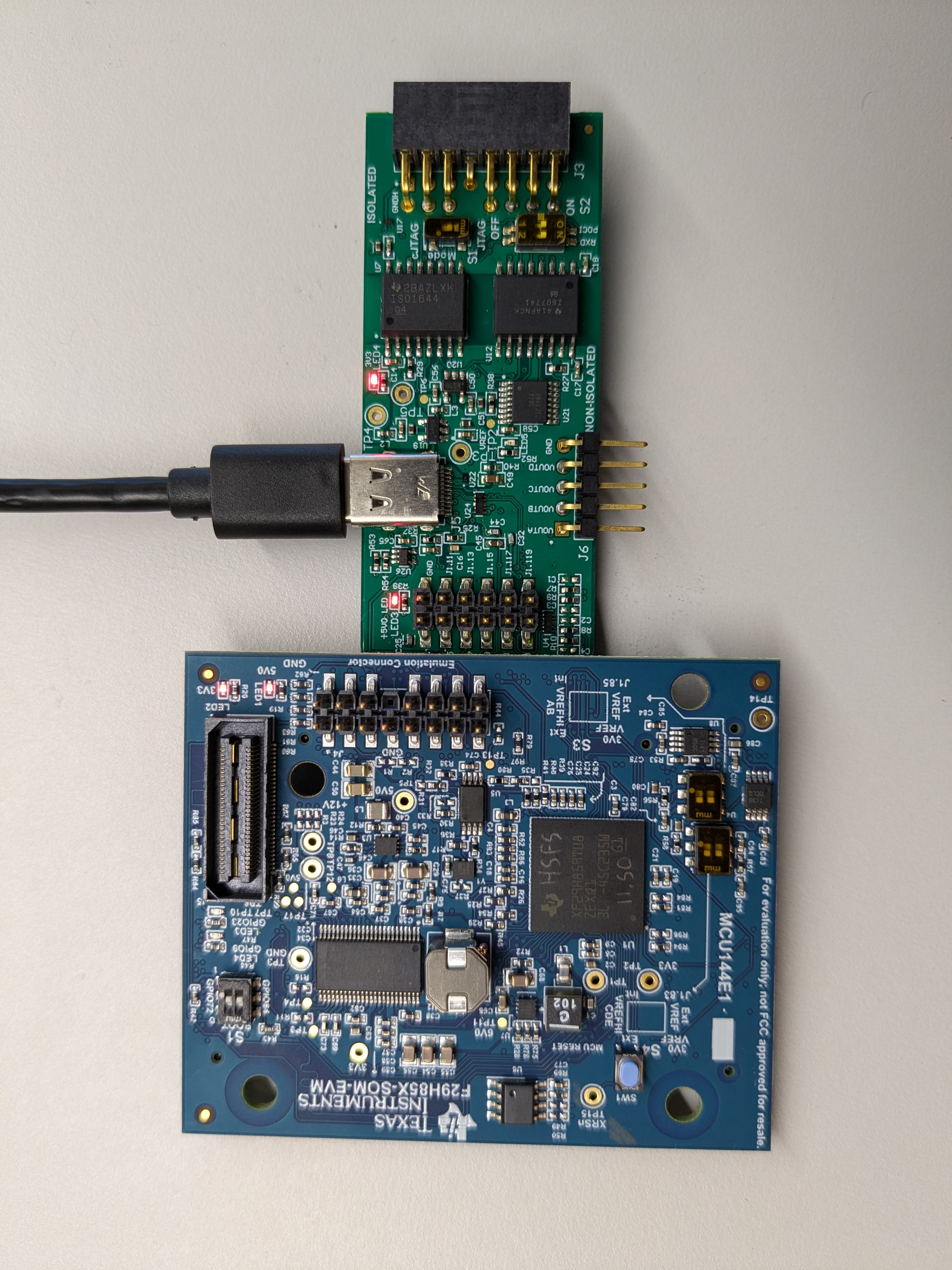
The stand-alone configuration can be used for most software development use cases which do not require the controlSOM to interface to other hardware. An XDS110 debug-probe (XDS110ISO-EVM) is required for this configuration. Power is provided to the controlSOM through XDS110 debug-probe. The XDS110 debug-probe is sold separately.
In this configuration, Code Composer Studio™ Theia connects to the controlSOM via JTAG and enables software development. The XDS110 debug-probe also enumerates a virtual COM port (VCP) for communication with the MCU via UART.
Follow these steps to enable this configuration:
- Collect the required equipment:
- F29H85x controlSOM (F29H85X-SOM-EVM)
- XDS110 isolated debug probe (XDS110ISO-EVM)
- USB Type-C® cable
- Verify the switch settings are correct on each EVM.
- F29H85X-SOM-EVM:
- Use S1 to select the desired boot mode.
- Use S3/S4 to select the desired ADC voltage reference mode.
- XDS110ISO-EVM: No switch configuration is necessary.
- F29H85X-SOM-EVM:
- Connect the XDS110ISO-EVM to connector J1 of the controlSOM.
- Connect the USB cable into connector J5 on the XDS110 isolated debug probe. The XDS110 isolated probe and the controlSOM are powered on.
- Verify the power status LEDs (LED1 and LED2) on the controlSOM are turned on.
- The controlSOM is ready for use. Follow the steps in Software to get started developing software.
 Figure 2-1 Stand-alone
Configuration
Figure 2-1 Stand-alone
ConfigurationIn the stand-alone configuration, the 12-pin prototype header (J2) on the XDS110ISO-EVM provides access a few ADC and GPIO pins on the F29H85x device. Table 2-1 lists the ADC and GPIO pins which can be accessed on this prototype header.
|
MCU Signal |
SOM Standard |
Pin |
Pin |
SOM Standard |
MCU Signal |
|---|---|---|---|---|---|
|
GND |
GND |
12 |
11 |
GND |
GND |
|
GPIO5 |
J1.5 |
10 |
9 |
J1.11 |
GPIO2 |
|
GPIO4 |
J1.7 |
8 |
7 |
J1.13 |
GPIO1 |
|
GPIO3 |
J1.9 |
6 |
5 |
J1.15 |
GPIO0 |
|
A7/E25/GPIO225/CMP9P/CMP2N |
J1.118 |
4 |
3 |
J1.117 |
A1/C25/CMP7P/CMP4N |
|
A6/E24/GPIO224/CMP2P/CMP12N |
J1.120 |
2 |
1 |
J1.119 |
A0/DACOUT1/C24/CMP4P/CMP9P |