SPRUJE4A August 2024 – November 2024 F29H850TU , F29H859TU-Q1
- 1
- Description
- Get Started
- Features
- 5
- 1Evaluation Module Overview
- 2Hardware
- 3Software
- 4Hardware Design Files
- 5Additional Information
- 6References
- 7Revision History
2.4.4 FSI DLT Support
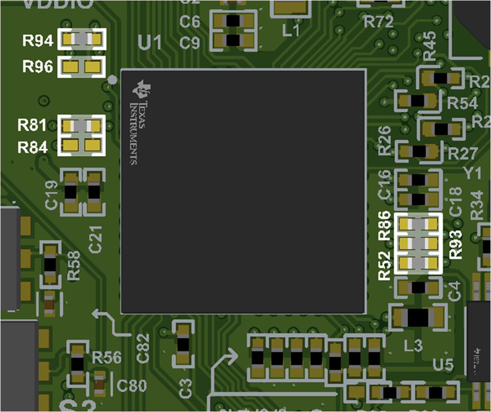
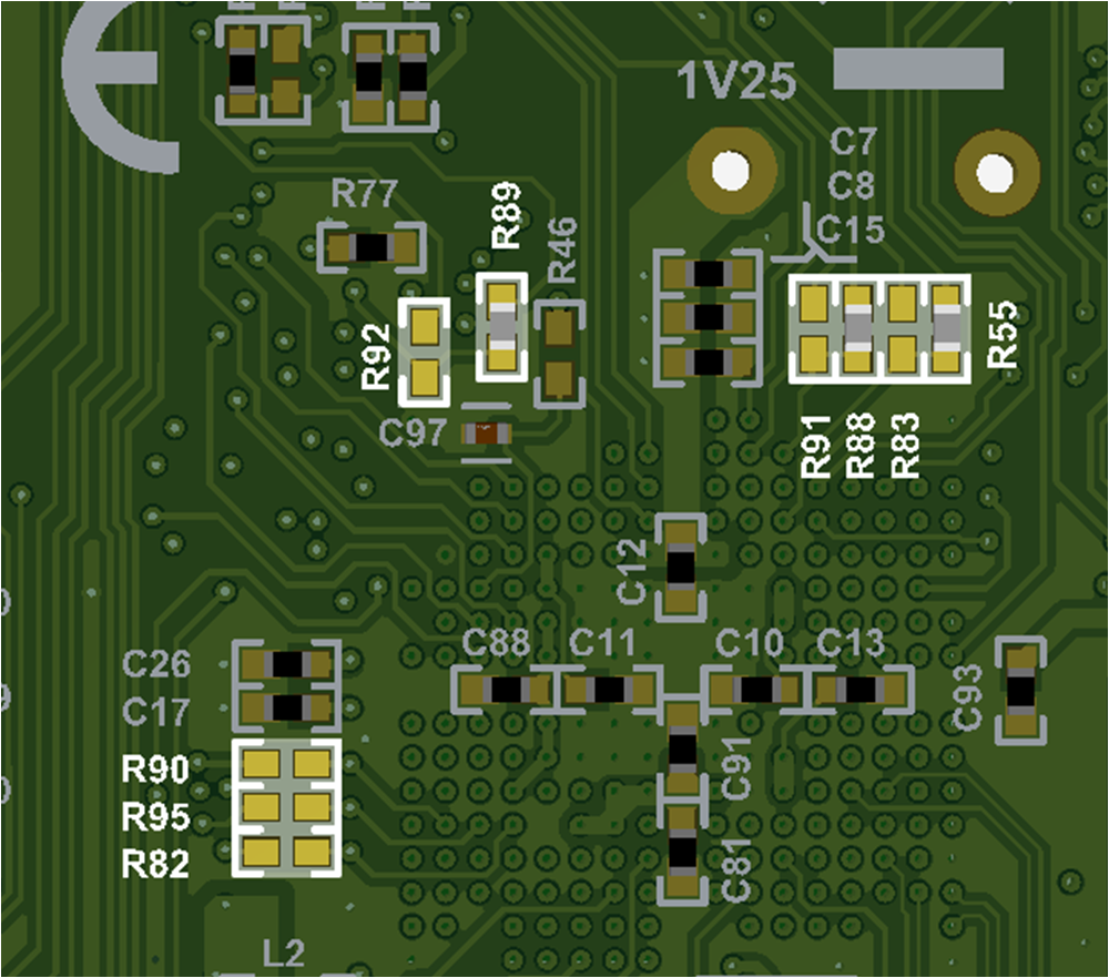
An optional resistor configuration is included on the F29H85x controlSOM to enable use of multiple FSI pins for data logging through the data, logging, and trace (DLT) header (J5). Table 2-7 lists all the FSI pins which can be connected to the DLT header. By default, these FSI pins are connected to the J1/J3 high-density connectors for baseboard use; they are not connected to the DLT header. To connect these FSI pins to the DLT header, follow the instructions on Table 2-8.
 Figure 2-11 FSI DLT Selection
Resistors
 Figure 2-12 FSI DLT Selection Resistor
Locations (Top)
 Figure 2-13 FSI DLT Selection Resistor
Locations (Bottom)
Figure 2-13 FSI DLT Selection Resistor
Locations (Bottom)|
GPIO |
Function |
|---|---|
|
GPIO51 |
FSITXA_CLK |
|
GPIO49 |
FSITXA_D0 |
|
GPIO50 |
FSITXA_D1 |
|
GPIO8 |
FSITXB_CLK |
|
GPIO6 |
FSITXB_D0 |
|
GPIO7 |
FSITXB_D1 |
|
GPIO16 |
FSIRXC_CLK |
|
GPIO76 |
FSIRXC_D0 |
|
Mode |
Resistor Configuration |
|---|---|
| FSI pins connected to J1/J3 Baseboard Headers (default) |
Populate all 0-ohm resistors on R52, R86, R93, R55, R88, R94, R81, and R89. Remove all resistors on R82, R90, R95, R83, R91, R96, R84, and R92. |
| FSI GPIOs connected to DLT Header |
Remove all resistors on R52, R86, R93, R55, R88, R94, R81, and R89. Populate all 0-ohm resistors on R82, R90, R95, R83, R91, R96, R84, and R92. |