SPRUJE4A August 2024 – November 2024 F29H850TU , F29H859TU-Q1
- 1
- Description
- Get Started
- Features
- 5
- 1Evaluation Module Overview
- 2Hardware
- 3Software
- 4Hardware Design Files
- 5Additional Information
- 6References
- 7Revision History
5.1.2 MCU144E1 Known Hardware Issues
ADC VREFHIAB and VREFHICDE incorrectly shorted together when S3 and S4 are both set to internal VREF mode
Switch S3 and S4 are used to specify the VREF mode for the VREFHIAB and VREFHICDE pins of the F29H85x microcontroller.
The VREFHIAB and VREFHICDE pins are incorrectly shorted together when internal VREF mode is selected on both S3 and S4. Refer to Section 2.4.2 for more information on S3 and S4.
A hardware modification is required to workaround this issue:
- Set S3/S4 for external mode
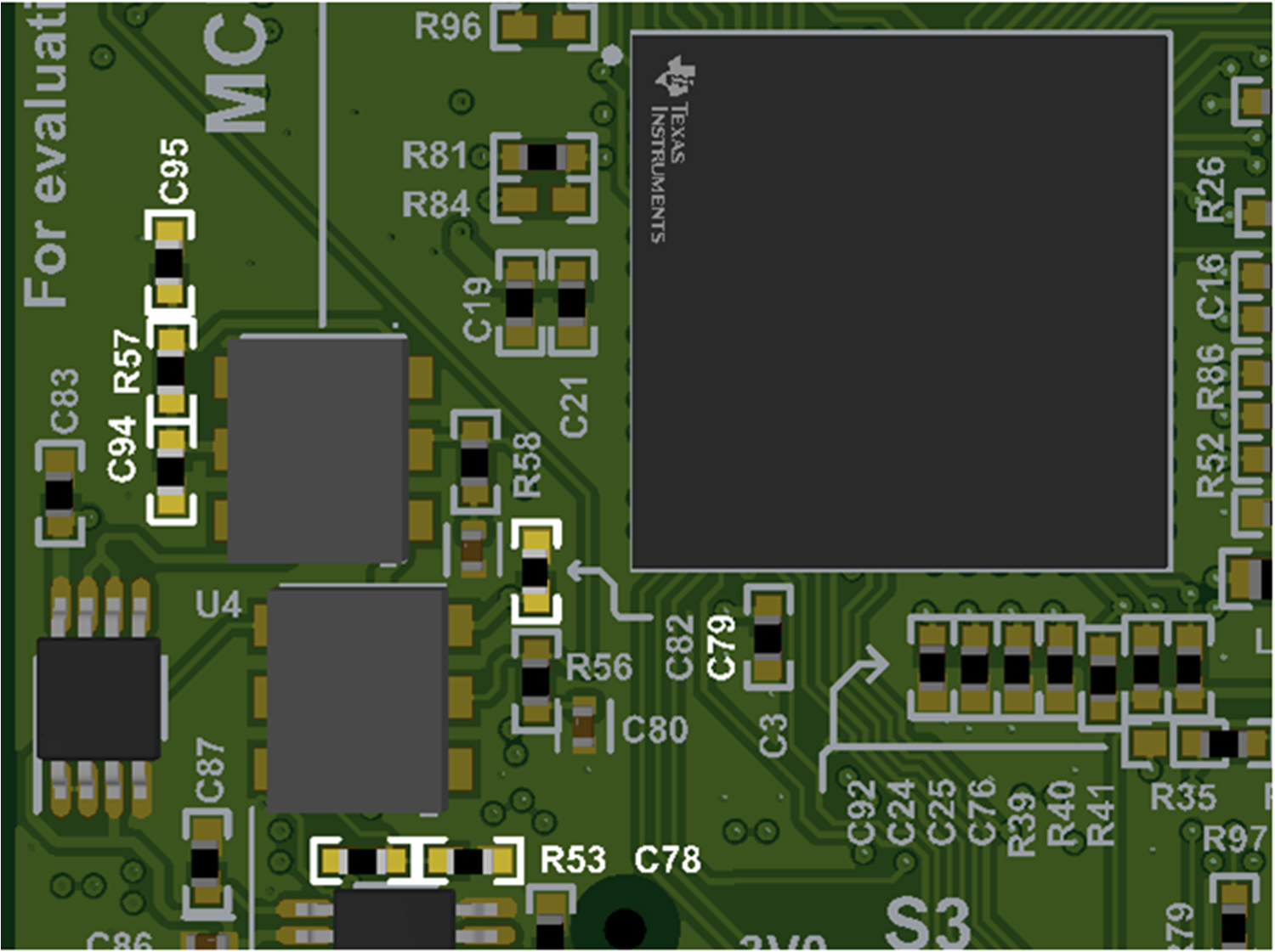
- Remove R53/C79
- Remove R57/C95
With this change the board will not drive any voltage on VREFHI pins. The ADCs can be used in internal VREF mode.
Incorrect voltage on VREFHIAB and VREFHICDE pins when external VREF mode is selected
Switch S3 and S4 are used to select the VREF mode for the VREFHIAB and VREFHICDE pins of the F29H85x microcontroller.
An incorrect voltage on the VREFHIAB and VREFHICDE will be observed when external VREF mode is selected.
A hardware modification is required to workaround this issue:
- Replace R53 and R57 on the on the board with 0-ohm resistors.
- Remove C78, C79, C94, and C95
 Figure 5-1 Component Location For ADC
VREF Modification
Figure 5-1 Component Location For ADC
VREF ModificationRefer to Section 2.4.2 for more information on S3 and S4.
Incorrect power-up sequence for VDD and VDDIO/VDDA MCU rails
The F29H85x and F29P58x Real-Time Microcontrollers data sheet specifies that the VDD rail should be powered-on after the VDDIO/VDDA rails have powered-on.
The power-management IC (PMIC) is programmed to bring up the VDD and VDDIO/VDD rails together. This incorrect power supply sequence can cause the MCU XRSn pin to remain asserted on some EVMs after power-on. On these boards, Code Compose Studio cannot connect to the MCU.
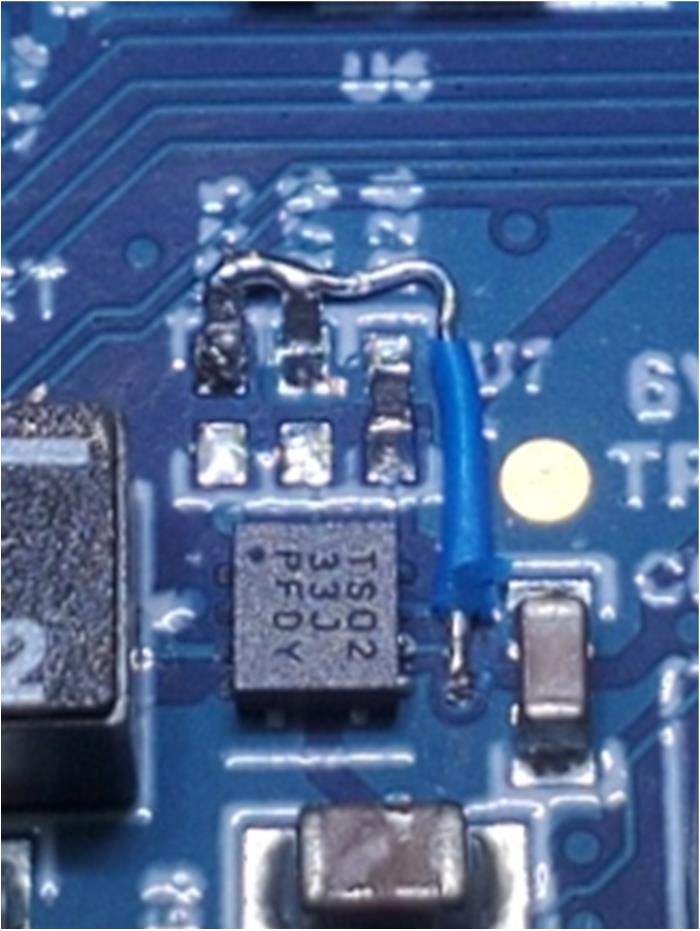
The hardware modification shown below is required to workaround this issue.
- Remove R22, R75, R78
- Add R1 and R2 as shown
- R1=10.7K (1%) R2=5760 (1%)
- Add blue wire between R1, R2, and U7.5 as shown
 Figure 5-2 Hardware Modification for
Power-Up Advisory
 Figure 5-3 Completed Modification for
Power-Up Advisory
Figure 5-3 Completed Modification for
Power-Up AdvisoryThis hardware modification has been implemented on all MCU144E1-002 assemblies.
FSI signals on the data logging and trace connector (J5) may interfere with some advanced debuggers
The data logging and trace (DLT) header (J5) includes various FSI signals for data logging.
The locations of these FSI signals on J5 may interfere with some advanced debuggers such as the XDS560v2.
By default the FSI signals are not connected to the DLT header (J5). Resistor modification is required to enable connection of the FSI signals to the DLT header.
Refer to Section 2.4.4 for more information on FSI signal support for DLT header.