SPRUJF1 November 2024 AM2612
ADVANCE INFORMATION
- 1
- Description
- Key Features
- 1LaunchPad Module Overview
-
2Hardware Description
- 3.1 Board Setup
- 3.2 Functional Block Diagram
- 3.3 GPIO Mapping
- 3.4 Reset
- 3.5 Clock
- 3.6 Memory Interfaces
- 3.7 Ethernet Interface
- 3.8 I2C
- 3.9 Industrial Application LEDs
- 3.10 SPI
- 3.11 UART
- 3.12 MCAN
- 3.13 FSI
- 3.14 JTAG
- 3.15 TIVA and Test Automation Pin Mapping
- 3.16 LIN
- 3.17 ADC and DAC
- 3.18 EQEP and SDFM
- 3.19 EPWM
- 3.20 USB
- 3.21 BoosterPack Headers
- 3Known Issues and modifications done on LP-AM261 RevE1
- 4Additional Information
- 5References
- 6Revision History
2.4 Reset
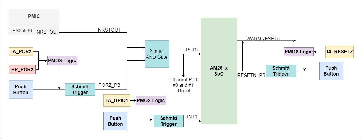
Figure 2-9 shows the reset architecture of the AM261x LaunchPad
 Figure 2-9 Reset
Architecture
Figure 2-9 Reset
ArchitectureThe AM261x LaunchPad has the following resets:
- PORz is the Power On Reset
- WARMRESETn is the warm reset
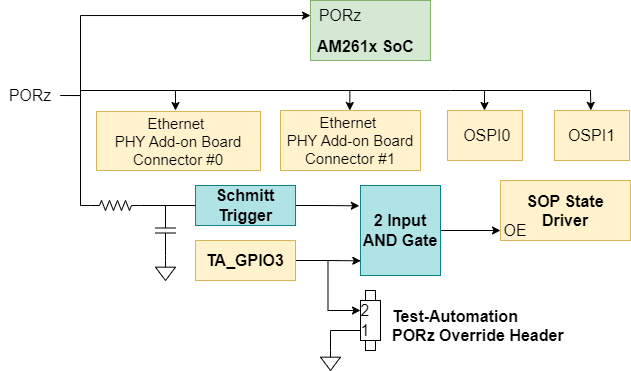
 Figure 2-10 PORZ Reset
Signal Tree
Figure 2-10 PORZ Reset
Signal TreeThe PORz signal is driven by a 2-input AND gate that generates a power on reset for the MAIN domain when:
- The PMIC's(TPS650360) NRSTOUT is driven low .
- The user push button (SW1) is pressed.
- A
P-Channel MOSFET gate's signal is logic LOW which
causes VGS of the PMOS to be less than
zero and so the PORz signal connects to the PMOS
drain which is tied directly to ground. The signals
that can create the logic LOW input to the PMOS gate
are:
- TA_PORZ output from the Test Automation header
- BP_PORZ output from either of the BoosterPack sites.
The PORz signal is tied to:
- AM261x SoC PORz input
- Both Ethernet port connector's reset input
- Both OSPI FLASH's reset input
- Boot mode
State Driver(U61)'s output enable input
- There is an RC filter to create a 1ms delay from GND to 3.0V such that the SOP State Driver's output enable input is low longer than the required SOP hold time following a PORz de-assertion.
The WARMRESETn signal creates a warm reset to the MAIN domain when:
- The user push button (SW2) is pressed.
The WARMRESETn signal is tied to:
- AM261x SoC WARMRESETN output
- RESETN_PB signal that is created from push button + PMOS logic
The AM261x LaunchPad also has an external interrupt to the SoC , INT1, that occurs when:
- The user push button (SW3) is pressed.