SPRUJF1 November   2024 AM2612

ADVANCE INFORMATION  

  1.   1
  2.   Description
  3.   Key Features
  4. 1LaunchPad Module Overview
    1. 2.1 Introduction
    2. 2.2 Preface: Read This First
      1. 2.2.1 If You Need Assistance
      2. 2.2.2 Important Usage Notes
    3. 2.3 Kit Contents
    4. 2.4 Device Information
      1. 2.4.1 System Architecture Overview
      2. 2.4.2 Security
      3. 2.4.3 Compliance
      4. 2.4.4 BoosterPacks
      5. 2.4.5 Component Identification
  5. 2Hardware Description
    1. 3.1  Board Setup
      1. 3.1.1 Power Requirements
        1. 3.1.1.1 Power Input Using USB Type-C Connector
        2. 3.1.1.2 Power Status LEDs
        3. 3.1.1.3 Power Tree
      2. 3.1.2 Push Buttons
      3. 3.1.3 Boot mode Selection
      4. 3.1.4 IO Expander
    2. 3.2  Functional Block Diagram
    3. 3.3  GPIO Mapping
    4. 3.4  Reset
    5. 3.5  Clock
    6. 3.6  Memory Interfaces
      1. 3.6.1 OSPI
      2. 3.6.2 Board ID EEPROM
    7. 3.7  Ethernet Interface
      1. 3.7.1 Ethernet PHY Add-on Board connector #0 - CPSW RGMII/ICSSM
      2. 3.7.2 Ethernet PHY Add-on Board connector #1 - CPSW RGMII/ICSSM
    8. 3.8  I2C
    9. 3.9  Industrial Application LEDs
    10. 3.10 SPI
    11. 3.11 UART
    12. 3.12 MCAN
    13. 3.13 FSI
    14. 3.14 JTAG
    15. 3.15 TIVA and Test Automation Pin Mapping
    16. 3.16 LIN
    17. 3.17 ADC and DAC
    18. 3.18 EQEP and SDFM
    19. 3.19 EPWM
    20. 3.20 USB
    21. 3.21 BoosterPack Headers
  6. 3Known Issues and modifications done on LP-AM261 RevE1
    1. 4.1 TA_POWERDOWNz pulled up by VSYS_TA_3V3 which is powered by VSYS_3V3
    2. 4.2 USB2.0_MUX_SEL0 pulled up by R355
    3. 4.3 MDIO and MDC of PRU0-ICSS0 needs to be routed to both Ethernet PHYs
    4. 4.4 AM261_RGMII1_RXLINK and AM261_RGMII2_RXLINK to be connected to GPIO
  7. 4Additional Information
    1.     Trademarks
    2. 5.1 Sitara MCU+ Academy
  8. 5References
    1. 6.1 Reference Documents
    2. 6.2 Other TI Components Used in This Design
    3. 6.3 Related Documentation From Texas Instruments
  9. 6Revision History

Ethernet PHY Add-on Board connector #1 - CPSW RGMII/ICSSM

Note: The PRU internal pinmux mapping provided in the TRM is part of the original hardware definition of the PRU. However, due to the flexibility provided by the IP and associated firmware configurations, this is not necessarily a hard requirement. The first PRU implementation for AM65x had the MII TX pins swapped during initial SOC integration and this convention was maintained for subsequent PRU revisions to enable firmware reuse. To make use of the SDK firmware, use the SYSCONFIG generated PRU pin mapping.

The AM261x LaunchPad has a 48-pin Ethernet PHY Add-on Board connector connected to either CPSW RGMII or one on-die Programmable Real-time Unit and Industrial Communication Sub System (PRU-ICSS). The RGMII CPSW port and ICSSM are internally pinmuxed on the AM261x SoC. For more information on the internal muxing of signals refer to Pinmux Mapping. AM261x internal Pinmux is used to select between the RGMII or PRU-ICSS signals. Ethernet port connector can be connected to the Ethernet daughtercard that comprises a PHY device and RJ45 connector.
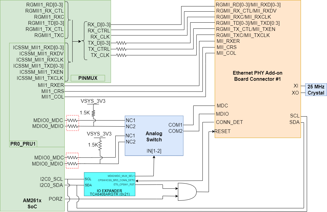
AM261x Ethernet PHY Add-on Board connector #1 Figure 2-15 Ethernet PHY Add-on Board connector #1

The MDIO signal from the SoC to the ethernet port connector requires 1.5kΩ pullup resistors to the 3.3V system supply voltage for proper operation. There is an analog switch (TS5A23159DGSR) that selects between the CPSW MDIO/MDC and the ICSSM MDIO/MDC signals to be routed to the Ethernet port connector. This analog switch is controlled by an IO expander signal that selects between CPSW MDIO/MDC and ICSSM MDIO/MDC signals.

The reset input for the PHY from Ethernet port connector is controlled by the PORz AM261x SoC output signal.