SPRUJF1 November 2024 AM2612
ADVANCE INFORMATION
- 1
- Description
- Key Features
- 1LaunchPad Module Overview
-
2Hardware Description
- 3.1 Board Setup
- 3.2 Functional Block Diagram
- 3.3 GPIO Mapping
- 3.4 Reset
- 3.5 Clock
- 3.6 Memory Interfaces
- 3.7 Ethernet Interface
- 3.8 I2C
- 3.9 Industrial Application LEDs
- 3.10 SPI
- 3.11 UART
- 3.12 MCAN
- 3.13 FSI
- 3.14 JTAG
- 3.15 TIVA and Test Automation Pin Mapping
- 3.16 LIN
- 3.17 ADC and DAC
- 3.18 EQEP and SDFM
- 3.19 EPWM
- 3.20 USB
- 3.21 BoosterPack Headers
- 3Known Issues and modifications done on LP-AM261 RevE1
- 4Additional Information
- 5References
- 6Revision History
2.17 ADC and DAC
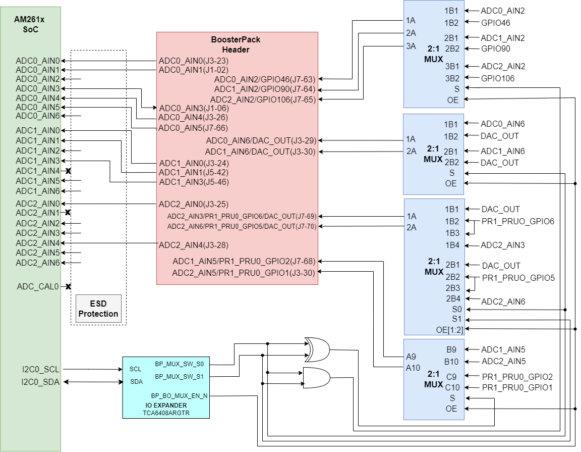
The AM261x LaunchPad maps 20 ADC inputs to the BoosterPack header. All of the ADC inputs that are used in the LaunchPad are ESD protected.
 Figure 2-24 ADC/DAC Signal Pathing
Multiple muxes are involved from AM261x Soc to BoosterPack connectors. Detailed table is given in Boosterpack section.
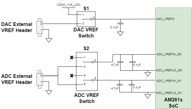
The ADC and DAC require a voltage reference. The AM261x LaunchPad has two switches that allow the user to switch between the DAC and ADC VREF source.
 Figure 2-25 ADC and DAC VREF Switches
The DAC VREF Switch (S1) is a single pole double throw switch that controls the input of the ADC VREF inputs of the AM261x SoC.
| DAC VREF Switch Position | Reference Selection |
|---|---|
| Pin 1-2 | AM261x on-die LDO |
| Pin 2-3 | External DAC VREF Header |
The ADC VREF Switch (S2) contains two single pole double throw switches that controls the input of the ADC VREF inputs of the AM261x SoC.
| ADC VREF Switch Position | Reference Selection |
|---|---|
| Pin 1-2 | OPEN - Allow for reference to be AM261x on-die LDO reference |
| Pin 2-3 | External ADC VREF Header |
| Pin 4-5 | OPEN - Allow for reference to be AM261x on-die LDO reference |
| Pin 5-6 | External ADC VREF Header |