SPRUJF1 November 2024 AM2612
ADVANCE INFORMATION
- 1
- Description
- Key Features
- 1LaunchPad Module Overview
-
2Hardware Description
- 3.1 Board Setup
- 3.2 Functional Block Diagram
- 3.3 GPIO Mapping
- 3.4 Reset
- 3.5 Clock
- 3.6 Memory Interfaces
- 3.7 Ethernet Interface
- 3.8 I2C
- 3.9 Industrial Application LEDs
- 3.10 SPI
- 3.11 UART
- 3.12 MCAN
- 3.13 FSI
- 3.14 JTAG
- 3.15 TIVA and Test Automation Pin Mapping
- 3.16 LIN
- 3.17 ADC and DAC
- 3.18 EQEP and SDFM
- 3.19 EPWM
- 3.20 USB
- 3.21 BoosterPack Headers
- 3Known Issues and modifications done on LP-AM261 RevE1
- 4Additional Information
- 5References
- 6Revision History
2.8 I2C
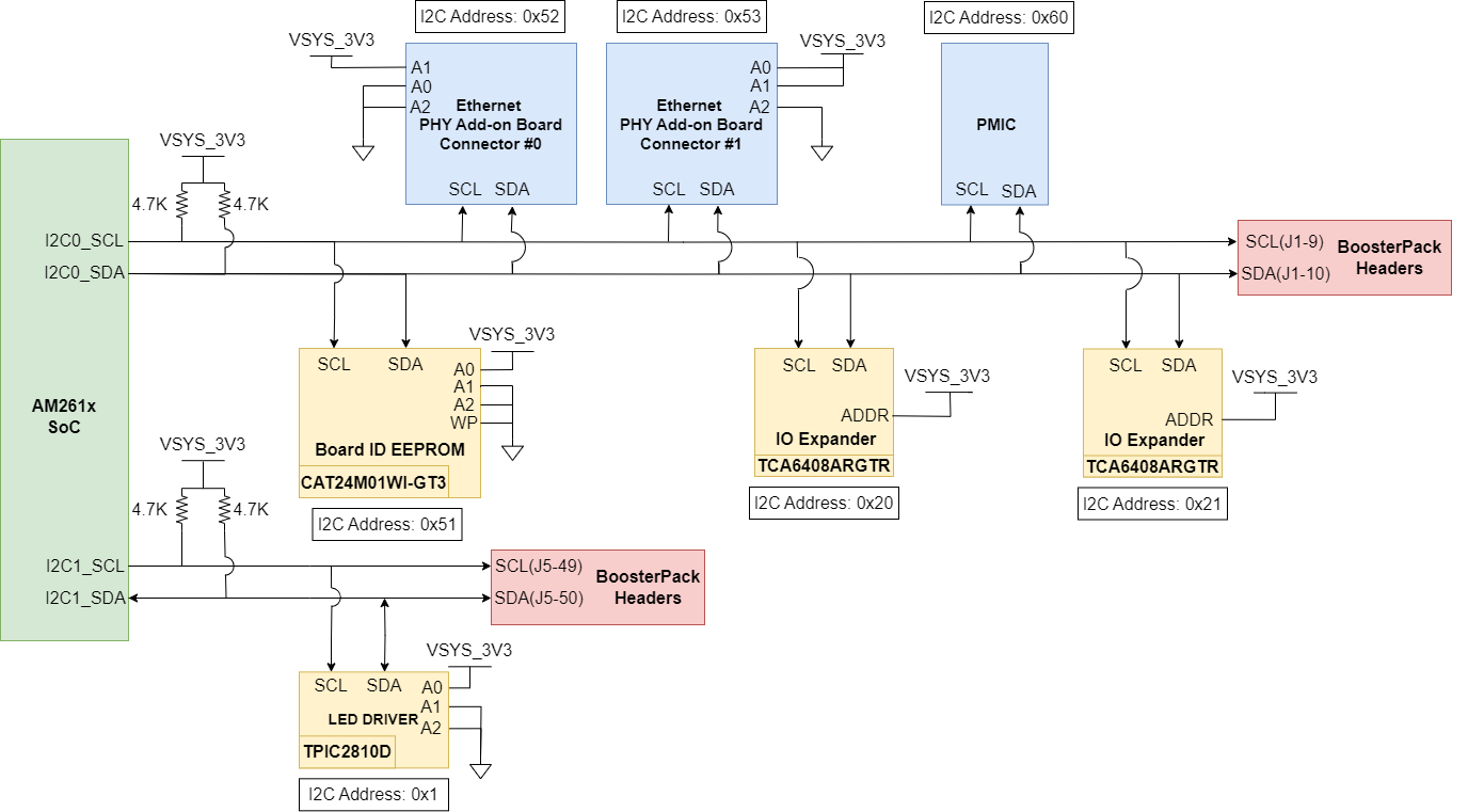
The AM261x LaunchPad uses two AM261x SoC inter-integrated circuit (I2C) ports to operate as a controller for various targets. I2C data and clock lines needs to be pulled up to the 3.3V system voltage supply to enable communication.
 Figure 2-16 I2C Targets
Table 2-7 I2C Addressing
| Target | I2C Instance | I2C Addres Bit Description | Device Addressing | LaunchPad Config. | I2C Address |
|---|---|---|---|---|---|
| Board ID EEPROM | I2C0 | The first 4 bits of the device address are set to 1010, the next two are set by the A2 and A1 pins, the seventh bit, a16, is the most significant internal address bit | 0b10110[A2][A1][a16] A1 and A2 is connected to ground |
0b1010001 | 0x51 |
| LED Driver | I2C1 | The first four bits of the target address are 0000, the following three are determined by A2, A1, and A0 | 0b0000[A2][A1][A0] A2 and A1 are connected to ground A0 is connected to 3.3V supply |
0b0000001 | 0x01 |
| BoosterPack Headers | I2C0, I2C1 |
Dependent on target | |||
| IO Expander #1 | I2C0 | The first 6 bits of the target address are set to 010000, the next bit is determined by the addr pin of the IO expander | IO_ADDR pin connected to 3.3V supply | 0b0100001 | 0x21 |
|
IO Expander #2 |
I2C0 | The first 6 bits of the target address are set to 010000, the next bit is determined by the addr pin of the IO expander | IO_ADDR pin connected to 3.3V supply | 0b0100000 | 0x20 |
| Ethernet PHY add-on Board Connector #0 | I2C0 | The first four bits of the target address are 1010, the following three are determined by A2, A1, and A0 | 0b1010[A2][1][A0] A2 and A0 are connected to ground |
0b1010010 | 0x52 |
| Ethernet PHY add-on Board Connector #1 | I2C0 | The first four bits of the target address are 1010, the following three are determined by A2, A1, and A0 | 0b1010[A2][1][A0] A2 are connected to ground and A0 is connected to 3.3V supply |
0b1010011 | 0x53 |
| PMIC | I2C0 | 7 bit device address for the PMIC is 1100000 | 0b1100000 | 0b1100000 | 0x60 |
Note: Underlined address bits are fixed based on the device addressing and cannot be configured.