SPRZ267J March 2009 – September 2020 TMS320C28341 , TMS320C28342 , TMS320C28343 , TMS320C28343-Q1 , TMS320C28344 , TMS320C28345 , TMS320C28346 , TMS320C28346-Q1
Advisory
FPU: FPU-to-CPU Register Move Operation Preceded by Any FPU 2p Operation
Revision(s) Affected
0
Details
This advisory applies when a multi-cycle (2p) FPU instruction is followed by a FPU-to-CPU register transfer. If the FPU-to-CPU read instruction source register is the same as the 2p instruction destination, then the read may be of the value of the FPU register before the 2p instruction completes. This occurs because the 2p instructions rely on data-forwarding of the result during the E3 phase of the pipeline. If a pipeline stall happens to occur in the E3 phase, the result does not get forwarded in time for the read instruction.
The 2p instructions impacted by this advisory are MPYF32, ADDF32, SUBF32, and MACF32. The destination of the FPU register read must be a CPU register (ACC, P, T, XAR0...XAR7). This advisory does not apply if the register read is a FPU-to-FPU register transfer.
In the example below, the 2p instruction, MPYF32, uses R6H as its destination. The FPU register read, MOV32, uses the same register, R6H, as its source, and a CPU register as the destination. If a stall occurs in the E3 pipeline phase, then MOV32 will read the value of R6H before the MPYF32 instruction completes.
Example of Problem:
   MPYF32 R6H, R5H, R0H  ; 2p FPU instruction that writes to R6H
|| MOV32 *XAR7++, R4H
   F32TOUI16R R3H, R4H   ; delay slot
   ADDF32 R2H, R2H, R0H
|| MOV32 *--SP, R2H      ; alignment cycle
   MOV32 @XAR3, R6H      ; FPU register read of R6H
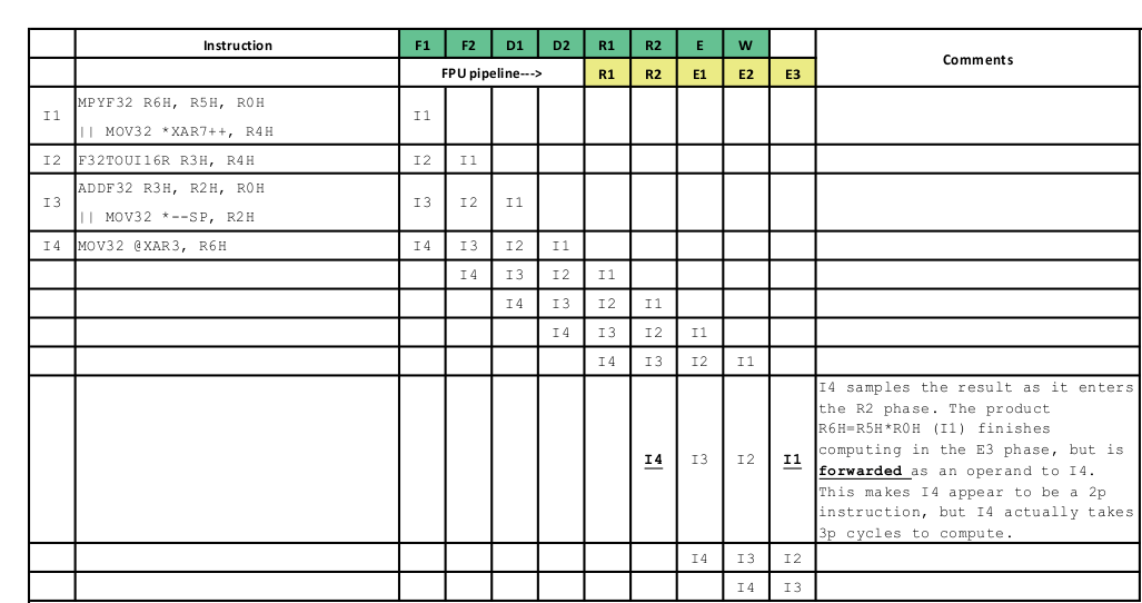
Figure 4-2 shows the pipeline diagram of the issue when there are no stalls in the pipeline.
 Figure 4-2 Pipeline Diagram of the Issue When
There are no Stalls in the Pipeline
Figure 4-2 Pipeline Diagram of the Issue When
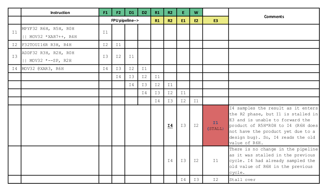
There are no Stalls in the PipelineFigure 4-3 shows the pipeline diagram of the issue if there is a stall in the E3 slot of the instruction I1.
 Figure 4-3 Pipeline Diagram of the Issue if
There is a Stall in the E3 Slot of the Instruction I1
Figure 4-3 Pipeline Diagram of the Issue if
There is a Stall in the E3 Slot of the Instruction I1Workaround(s)
Treat MPYF32, ADDF32, SUBF32, and MACF32 in this scenario as 3p-cycle instructions. Three NOPs or non-conflicting instructions must be placed in the delay slot of the instruction.
The C28x Code Generation Tools v.6.2.0 and later will both generate the correct instruction sequence and detect the error in assembly code. In previous versions, v6.0.5 (for the 6.0.x branch) and v.6.1.2 (for the 6.1.x branch), the compiler will generate the correct instruction sequence but the assembler will not detect the error in assembly code.
Example of Workaround:
   MPYF32 R6H, R5H, R0H
|| MOV32 *XAR7++, R4H     ; 3p FPU instruction that writes to R6H
   F32TOUI16R R3H, R4H    ; delay slot
   ADDF32 R2H, R2H, R0H
|| MOV32 *--SP, R2H       ; delay slot
   NOP                    ; alignment cycle
   MOV32 @XAR3, R6H       ; FPU register read of R6H
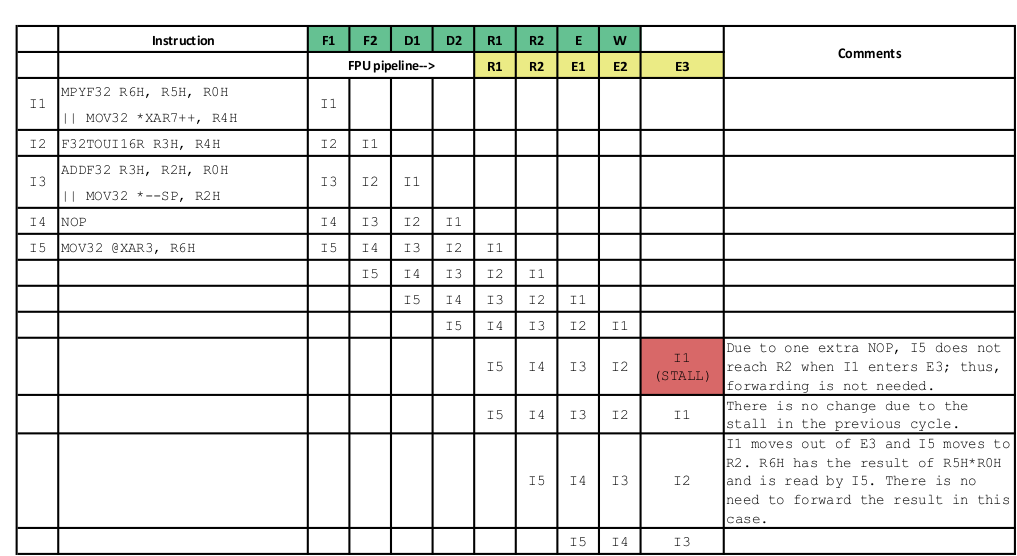
Figure 4-4 shows the pipeline diagram with the workaround in place.
 Figure 4-4 Pipeline Diagram With Workaround
in Place