SPRZ439H January 2017 – February 2024 TMS320F280040-Q1 , TMS320F280040C-Q1 , TMS320F280041 , TMS320F280041-Q1 , TMS320F280041C , TMS320F280041C-Q1 , TMS320F280045 , TMS320F280048-Q1 , TMS320F280048C-Q1 , TMS320F280049 , TMS320F280049-Q1 , TMS320F280049C , TMS320F280049C-Q1
- 1
- TMS320F28004x Real-Time MCUs Silicon Errata (Silicon Revisions B, A, 0)
- 1Usage Notes and Advisories Matrices
- 2Nomenclature, Package Symbolization, and Revision Identification
-
3Silicon Revision B Usage Notes and
Advisories
- 3.1
Silicon Revision B Usage Notes
- 3.1.1 PIE: Spurious Nested Interrupt After Back-to-Back PIEACK Write and Manual CPU Interrupt Mask Clear
- 3.1.2 FPU32 and VCU Back-to-Back Memory Accesses
- 3.1.3 Caution While Using Nested Interrupts
- 3.1.4 Security: The primary layer of defense is securing the boundary of the chip, which begins with enabling JTAGLOCK and Zero-pin Boot to Flash feature
- 3.2
Silicon Revision B Advisories
- Advisory
- Advisory
- Advisory
- Advisory
- Advisory
- Advisory
- Advisory
- Advisory
- Advisory
- Advisory
- Advisory
- Advisory
- Advisory
- Advisory
- Advisory
- Advisory
- 3.2.1 Advisory
- Advisory
- Advisory
- Advisory
- Advisory
- 3.2.2 Advisory
- Advisory
- Advisory
- Advisory
- Advisory
- Advisory
- 3.2.3 Advisory
- Advisory
- Advisory
- 3.2.4 Advisory
- 3.1
Silicon Revision B Usage Notes
- 4Silicon Revision A Usage Notes and Advisories
- 5Silicon Revision 0 Usage Notes and Advisories
- 6Documentation Support
- 7Trademarks
- 8Revision History
Advisory
I2C: SDA and SCL Open-Drain Output Buffer Issue
Revisions Affected
0, A, B
Details
The SDA and SCL outputs are implemented with push-pull 3-state output buffers rather than open-drain output buffers as required by I2C. While it is possible for the push-pull 3-state output buffers to behave as open-drain outputs, an internal timing skew issue causes the outputs to drive a logic-high for a duration of 0–5 ns before the outputs are disabled. The unexpected high-level pulse will only occur when the SCL or SDA outputs transition from a driven low state to a high-impedance state and there is sufficient internal timing skew on the respective I2C output.
This short high-level pulse injects energy in the I2C signals traces, which causes the I2C signals to sustain a period of ringing as a result of multiple transmission line reflections. This ringing should not cause an issue on the SDA signal because it only occurs at times when SDA is expected to be changing logic levels and the ringing will have time to damp before data is latched by the receiving device. The ringing may have enough amplitude to cross the SCL input buffer switching threshold several times during the first few nanoseconds of this ringing period, which may cause clock glitches. This ringing should not cause a problem if the amplitude is damped within the first 50 ns because I2C devices are required to filter their SCL inputs to remove clock glitches. Therefore, it is important to design the PCB signal traces to limit the duration of the ringing to less than 50 ns. One possible solution is to insert series termination resistors near the SCL and SDA terminals to attenuate transmission line reflections.
This issue may also cause the SDA output to be in contention with the slave SDA output for the duration of the unexpected high-level pulse when the slave begins its ACK cycle. This occurs because the slave may already be driving SDA low before the unexpected high-level pulse occurs. The glitch that occurs on SDA as a result of this short period of contention does not cause any I2C protocol issue but the peak current applies unwanted stress to both I2C devices and potentially increases power supply noise. Therefore, a series termination resistor located near the respective SDA terminal is required to limit the current during the short period of contention.
A similar contention problem can occur on SCL when connected to I2C slave devices that support clock stretching. This occurs because the slave is driving SCL low before the unexpected high-level pulse occurs. The glitch that occurs on SCL as a result of this short period of contention does not cause any I2C protocol issue because I2C devices are required to apply a glitch filter to their SCL inputs. However, the peak current applies unwanted stress to both I2C devices and potentially increases power supply noise. Therefore, a series termination resistor located near the respective SCL terminal is required to limit the current during the short period of contention.
If another master is connected, the unexpected high-level pulses on the SCL and SDA outputs can cause contention during clock synchronization and arbitration. The series termination resistors described above will also limit the contention current in this use case without creating any I2C protocol issue.
Workaround
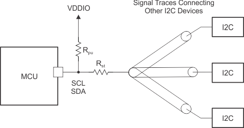
Insert series termination resistors on the SCL and SDA signals and locate them near the SCL and SDA terminals. The SCL and SDA pullup resistors should also be located near the SCL and SDA terminals. The placement of the series termination resistor and pullup resistor should be connected as shown in Figure 3-4.
 Figure 3-4 Placement of Series
Termination Resistor and Pullup Resistor