SPRZ454B February 2018 – September 2024 TDA2P-ABZ , TDA2P-ACD
- 1
- 1Introduction
-
2Silicon Advisories
- Revisions SR 1.0 - Advisories List
- i202
- i378
- i631
- i694
- i698
- i699
- i709
- i727
- i729
- i734
- i767
- i782
- i783
- i802
- i803
- i807
- i808
- i809
- i810
- i813
- i814
- i815
- i818
- i819
- i820
- i824
- i826
- i829
- i834
- i849
- i856
- i862
- i863
- i869
- i870
- i871
- i872
- i874
- i878
- i879
- i883
- i889
- i890
- i893
- i896
- i897
- i898
- i899
- i900
- i903
- i904
- i916
- i929
- i930
- i932
- i933
- i936
- i940
- i2446
- 3Silicon Limitations
- 4Silicon Cautions
- 5Revision History
i864
VDDS18V to VDDSHVn Current Path
CRITICALITY
Medium
DESCRIPTION
A current path exists between vdds18v and vddshvn during power down sequence.
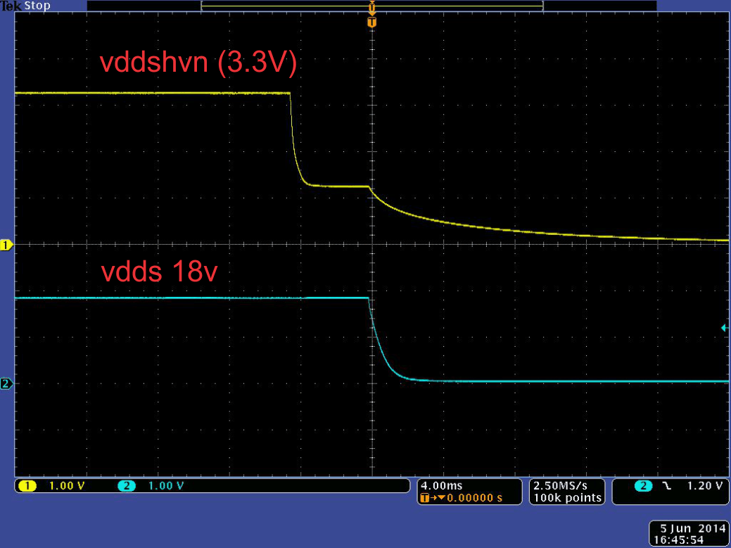
The Data Manual allows the vddshvn rail (in either 3.3V or 1.8V mode) to power down at the same time or before the vdds18v rail. When the vddshvn rail is powered down before the vdds18v rail, the vddshvn rail stays at Plateau Level (<1.5V) until the vdds18v rail is disabled, as shown in the waveform below.
A subset of the SOC's LVCMOS IOs (refer to DM for details) have a pull-up resistor that is active by default, including during reset and power-down. The SOC's IOs that have internal or external pull-ups will stay at Plateau Level (<1.5V) during the power-down. If other ICs on the board that are interfaced to the SOC's LVCMOS signals use a separate supply then it's possible that the other IC's signals can be pulled to the Plateau Level while its power supply is off.
 Figure 4-1 PAB_RevA
The root cause of the plateau is related to the LVCMOS IO buffer Dual Voltage detection circuitry. The LVCMOS Dual Voltage IO includes voltage comparator circuitry to determine if the IO is in 3.3V mode or 1.8V mode. During powerdown of vddshvn domains, a current path in the internal bias transistors results in the vddshvn rail being held to an intermediate voltage level (<1.5 V). This path can consume at most 500 uA per IO - worst case estimate is ~150 mA (based on 280 IOs) from the vdds18v supply during power down. This path is not a reliability concern for the device.
The plateau is no concern for systems where the same supply/LDO is used for vddshvn rail and the other components that interface to the SOC's Dual Voltage LVCMOS IOs.
Systems that use independent supplies for the SOC rail and the other component's rail require further analysis by the system designer. There may be a state where SOC's IO's with internal or external pull-ups are pulled to plateau level (<1.5V) while the external device is powered down. In this case, the current on any given IO is limited due to the ~10 kOhm (minimum) internal pull-up resistor. The limit is 150 uA per IO (1.5 V maximum plateau / 10 kOhm minimum pull-up resistor.) Refer to the device Data Manual for details on which pins include a pull-up resistor by default.
GUIDELINES
In general, TI recommends using the same supply source for connected components. E.g., a single LDO should drive vddshvn and the related 3.3V external components.
For systems that use a different 3.3V supply for the SOC and connected ICs, customers should evaluate their system for reliability risk. If necessary, the PMIC OTP power-down sequence can be modified to delay the vddshv[11:1] powerdown to coincide with the vdds18v powerdown. [Note: The 3.3V rail must never be 2.0V above the 1.8V rail.]
VDDSHV8 is a special case. If VDDSHV8 is powered by the same LDO/switch as the other VDDSHVn rails then the VDDSHV8 rail can also be delayed. However, if the VDDSHV8 rail is supplied by a different LDO (e.g., LDO1 on EVM) than the other VDDSHVn rails, then the sequence should not be modified.
REVISIONS IMPACTED
SR 1.0
AM574x: 1.0
DRA75xP, DRA74xP, DRA77xP, DRA76xP: 1.0
TDA2Px: 1.0
AM576x: 1.0