SSZT062 october 2022 LMG3410R070 , LMG3522R030

The growing market trend for electrification and the expansion of the electric vehicle industry present new challenges to the battery formation and test market, which remains the biggest bottleneck for the mass production of lithium-ion batteries. In response, design engineers are looking for ways to increase the channel density of test equipment, improve overall system efficiency, and decrease system cost. One such solution is gallium nitride (GaN) technology. In this article, I’ll explain how the implementation of GaN into battery test systems can help increase channel density, improve overall system efficiency, and decrease electricity costs, leading to a higher throughput of batteries from the testing factory.
Taking a Closer Look at Battery Test Systems
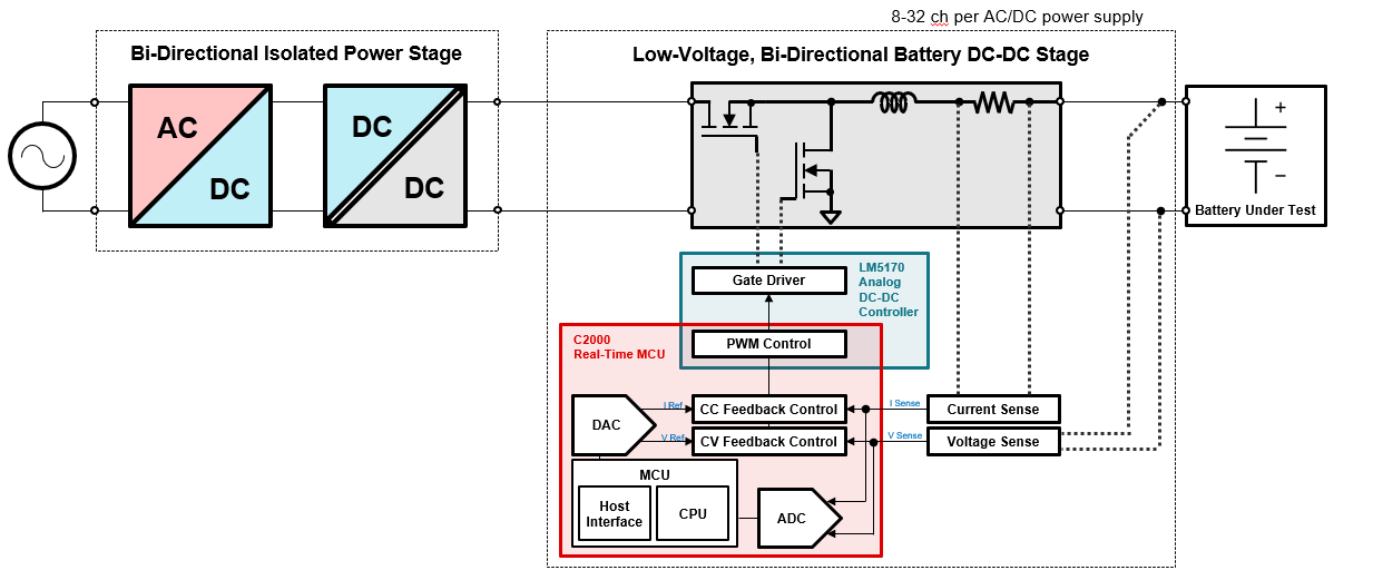
Battery test equipment charges and discharges cells during battery production. Figure 1 shows a block diagram of a common battery test system, consisting of a bidirectional isolated AC/DC power supply and multiple precision low-voltage output test channels.
 Figure 1 A Battery Test System Block
Diagram
Figure 1 A Battery Test System Block
DiagramMost battery test systems use bidirectional AC/DC power supplies, which often comprises an AC/DC non-isolated power factor correction (PFC) stage and an isolated DC/DC stage. There are two main challenges with this power supply type: size and efficiency. The power supply can take up to 40% of cabinet space, limiting the channel density of the test equipment. Factors such as switching and conduction losses, reverse-recovery losses, and power dissipation decrease the system’s overall efficiency, which in turn leads to higher electricity bills and an increased cost of battery production.
Increasing Efficiency in the AC/DC Stage with Totem-pole PFC
Many high-voltage applications have already adopted GaN transistors for the benefits they deliver in power density, efficiency, switching speed and frequency. Because of its low terminal capacitances and lack of third-quadrant reverse-recovery losses, GaN enables higher-frequency hard-switched topologies that are not possible with metal-oxide semiconductor field-effect transistors (MOSFETs) and isolated-gate bipolar transistors, such as the totem-pole bridgeless PFC stage. Figure 2 compares PFC topologies.
 Figure 2 Totem-pole PFC Compared to
Other Common PFC Topologies
Figure 2 Totem-pole PFC Compared to
Other Common PFC TopologiesAs the demand for higher efficiency in AC/DC power supplies grows, totem-pole PFC has become an increasingly valuable PFC solution given its low component count, low losses and higher power density. Since GaN has zero reverse-recovery losses, it is the best power transistor to implement in a totem-pole PFC stage. The 4-kW Single-Phase Totem Pole Reference Design with C2000™ and GaN shows an example implementation of a totem-pole PFC topology using GaN, operating at 4 kW with a peak efficiency of ≥99.1%. Totem-pole PFC is a good fit for applications that need high efficiency, such as in server power supplies, onboard chargers for electric vehicles, test and measurement systems, and grid infrastructures.
Improving Channel Density with GaN
GaN can operate at higher frequencies in a smaller form factor compared to silicon carbide FETs or MOSFETs, which is especially important for bidirectional AC/DC power supplies in the battery tester, since it then becomes possible to use that additional cabinet space to increase the number of precision low-voltage test channels. GaN allows an approximate 50% size reduction in the AC/DC stage compared to MOSFET solutions, which can enable an approximate 30% increase in channel density. In the GaN-Based, 6.6-kW, Bidirectional, Onboard Charger Reference Design, which uses the LMG3522R030 GaN FET, GaN enables higher power density and efficiency at a much smaller form factor than a comparable SiC reference design. Implementing GaN allows for a 62% higher switching frequency than SiC, all while maintaining an approximate 60% size reduction when compared to an equivalent SiC design.
Because of its higher switching frequency, GaN also enables a faster charge-to-discharge transition (<1 ms) than SiC and MOSFETs. Overall, by using GaN, you can increase the throughput of battery production in factories without compromising power density, efficiency and transient performance. Implementing GaN can help enable a reduction of bottlenecking at the battery formation stage, allowing for a more productive factory.
Increasing Reliability of Battery Test Designs
Reliability is extremely important in battery test systems; factories run year-round, so the need for a reliable power supply is paramount. GaN FETs benefit from standard reliability testing methods that have existed for silicon FETs and, in addition, new methodologies that have been implemented specifically to validate GaN FET reliability.
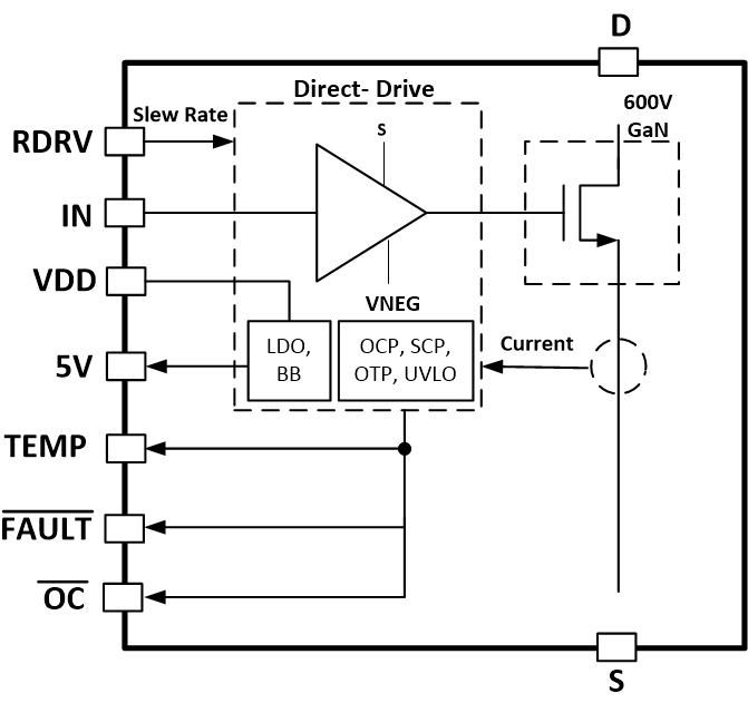
TI’s portfolio of GaN FETs includes a variety of built-in features for protection, leading to cost and reliability advantages. These features, as well as over 40 million hours of reliability testing, allow TI GaN packages to offer a resilient design. Some of the features included in the package are an integrated gate driver, overtemperature reporting and options for overcurrent protection. No external circuitry is necessary for these features, which saves on cost. Figure 3 is a block diagram of the LMG3422 and LMG3522 devices.
 Figure 3 LMG3422 and LMG3522 Block
Diagram
Figure 3 LMG3422 and LMG3522 Block
DiagramMinimizing Power Losses in the Isolated DC/DC Stage
GaN also presents advantages for battery test systems in factories that are moving to a centralized high-power AC/DC stage and running an 800-VDC rail. This architecture implements a single-stage 800-V to 12-V isolated DC/DC stage to step down the DC rail voltage and then step down to 0 V to 5 V using a non-isolated bidirectional buck converter to test the battery. Implementing GaN in the 800-V to 12-V isolated DC/DC stage reduces power losses when compared to SiC solutions. Multiple DC/DC converters would be tied to the 800-VDC bus, depending on the number of testing channels.
Conclusion
Many server power and telecom applications have successfully adopted GaN, benefiting from higher efficiency and power density. Battery test engineers can reap similar benefits by considering GaN for their designs to decrease electricity costs, increase channel density, and achieve a reliable GaN FET for their system application.
Additional Resources
- Read these white papers:
- Check out these technical articles:
- Download design files for the Bidirectional High Density GaN CCM Totem Pole PFC Using C2000 MCU reference design, which features bidirectionality and phase shedding for further efficiency improvements using the LMG3410R070 GaN power stage.