SSZT209 December 2020 TPSM41615 , TPSM41625 , TPSM5D1806 , TPSM846C23
Noise is an unwelcomed electrical phenomenon that commonly originates in the power supply. If not reduced, noise can adversely impact the performance of applications in sensitive medical, test and measurement, and aerospace and defense systems.
Today’s high-precision analog signal-chain systems require DC/DC switching regulators to generate regulated power-supply rails for powering analog-to-digital converters (ADCs), digital-to-analog converters (DACs), field-programmable grid arrays (FPGAs) and their subsystems in low-noise applications. While DC/DC switching regulators are efficient, their switching action results in large discontinuous currents, which generate high input and output voltage ripples, frequency spikes and wideband noise. If not controlled to the ADC or DAC’s least-significant-bit millivolt range, these discontinuous currents can affect system accuracy.
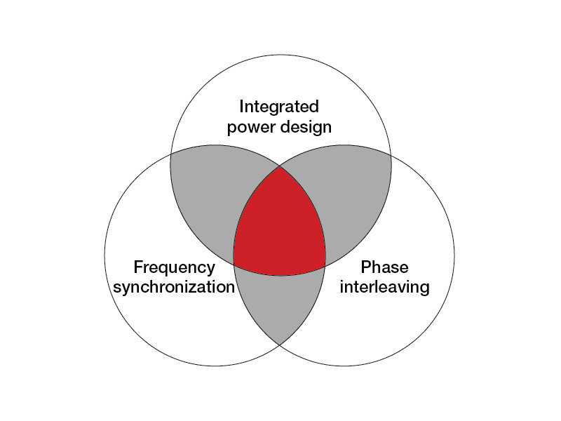
This article focuses on three ways that buck power modules can help with noise reduction: removing parasitics through an integrated module design, mitigating undesired beat frequency and inaccuracies with frequency synchronization, and lowering the input ripple current and output voltage ripple through phase interleaving. DC/DC buck power modules with all three features, as shown in Figure 1, can help significantly lower the noise of your power supply for low-noise applications.
 Figure 1 Venn diagram of desirable
DC/DC buck module features for low noise
Figure 1 Venn diagram of desirable
DC/DC buck module features for low noiseRemoving parasitics through an integrated module design
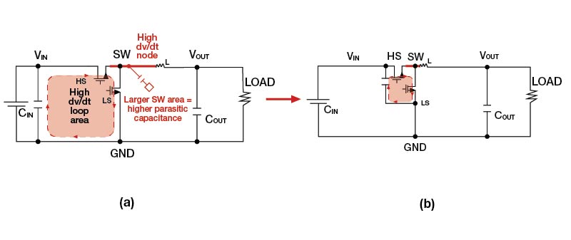
 Figure 2 The di/dt loop for a discrete converter (a) vs. a buck power module (b)
Mitigating undesired beat frequency and inaccuracies with frequency synchronization
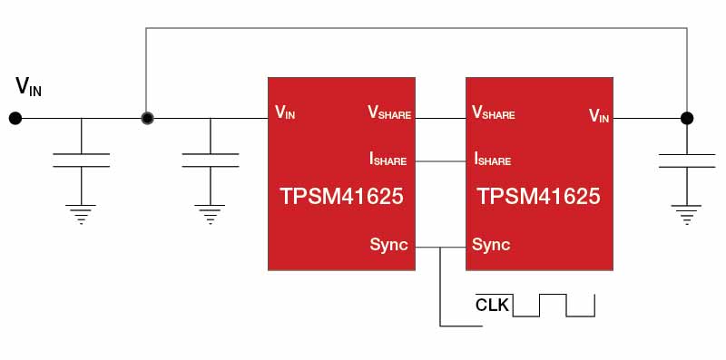
 Figure 3 Two buck power modules synchronized to a system clock
Lowering the input ripple current and output voltage ripple through phase interleaving
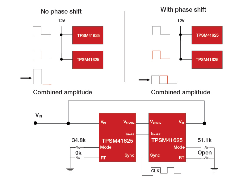
 Figure 4 A 180-Degree Phase-shift Synchronized TPSM41625 Modules
Conclusion
Additional resources
- Check out these application notes to learn more:
- Learn more about multiphase buck converters in the Analog Design Journal article, “Benefits of a multiphase buck converter.”