SSZT244 october 2020 ADC12DJ3200 , ADC12DJ5200RF , ADC12QJ1600-Q1
Whether you’re designing an aerospace and defense system, test and measurement equipment or automotive lidar analog front end (AFE), hardware designers using modern high-speed data converters face tough challenges with high-frequency inputs, outputs, clock rates and digital interface. Issues might include connecting with your field-programmable gate array (FPGA), being confident that your first design pass will work or determining how to best model the system before building it.
In this article, I’ll take a closer look at each of these challenges.
Rapid system development
Before starting a new hardware design, engineers often evaluate the most important chips on their own test bench. Once you have obtained the equipment necessary for running the typical evaluation board, component evaluation usually occurs with very idealistic supplies and signal sources. What TI has done in most cases is provide onboard power and clocking so that you can begin running the board with minimal test bench equipment and more realistic power supplies and signal sources, such as the setup shown in Figure 1.
 Figure 1 Typical ADC evaluation board
Once you have validated the performance, you can use the schematics and layout of the more complete evaluation board as a reference design for that portion of the subsystem. Our data-capture and pattern-generation tools support CMOS, LVDS, and JESD204, and come with the software needed to operate them. Using the evaluation board user’s guide for your high-speed data converter, it’s possible to get most boards up and running in less than 10 minutes. See Figure 2.
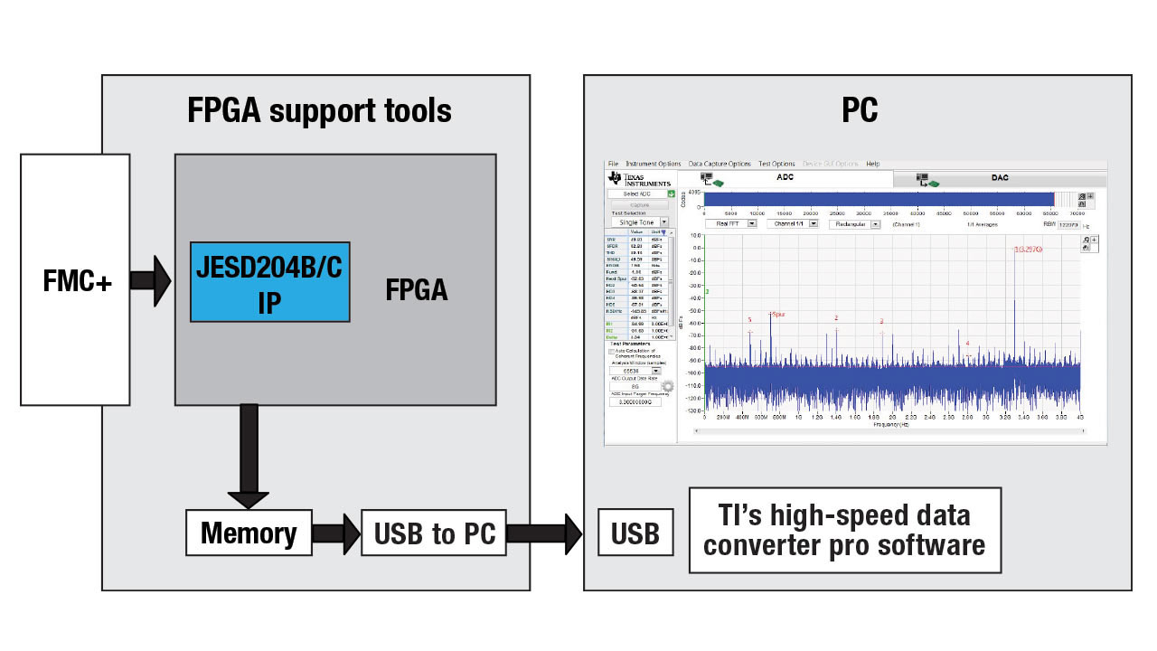 Figure 2 TI’s data-capture and pattern-generation hardware and software
As systems become more complicated, you may need to evaluate across a broader range of use cases. An evaluation board can help. If your evaluation needs become complex, you can use Python, Matlab, Labview or C++ software to directly communicate with the device through the device evaluation board, the capture card solution and the test-bench equipment. Great examples of support boards are the TSW1400EVM for LVDS/CMOS or the TSW14J56EVM for supporting JESD204B serializer-deserializer (SERDES) protocol devices, as shown in Figure 3.
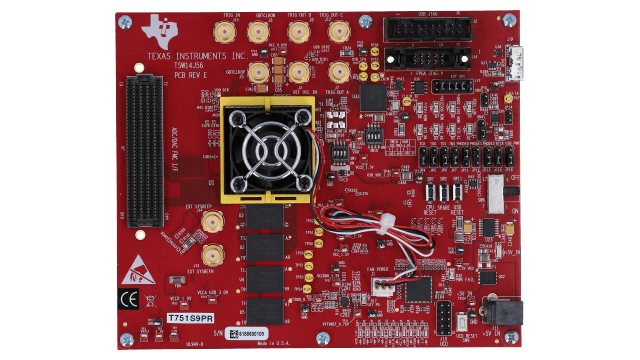 Figure 3 TI’s TSW14J56EVM for JESD204B data capture or pattern generation
TI also supports a complete system-level mockup of a multievaluation module prototype from a single PC. For example, it is possible to test transmit-and-receive channels simultaneously by connecting a Xilinx FPGA development kit like the KCU105 or VCU118 to multiple analog-to-digital converters (ADCs) or digital-to-analog converters (DACs).
| Accelerate your design from concept to prototype. | |
|
Explore our JESD204 Rapid Design IP to ease FPGA integration and cut overall development time. |
FPGA connectivity and JESD204B and JESD204C
One of the biggest problems you may have to solve is how to get data to and from your FPGA. While LVDS and CMOS are simple interfaces, they are very limited in the speed they can support per pin on the device. With newer high-speed data converters more commonly supporting input or output rates >1 GSPS, these interfaces either run out of steam or become not-so-simple to design with.
JEDEC, which develops open standards for the microelectronics industry, created JESD204 to solve this problem by supporting differential-pair lane rates beyond 12.5 Gbps. But while JESD204 minimizes the number of pins, it does drive up the interface complexity by encoding and serializing, or deserializing and decoding, parallel data.
Up until now, you have primarily had to rely on JESD204 intellectual property (IP) blocks and support offered by FPGA vendors. While these IP blocks do work very well, they are provided in a manner to support any device in any configuration. This means that they can be difficult to learn and configure for your specific use case. You either have to spend a great amount of effort designing the IP yourself, or seek the IP from a third-party IP provider. However, the third-party IP will require help and support in implementation if things go wrong.
Our JESD204 Rapid Design IP is pre-configurable and optimizable specifically for your FPGA platform, data converter and JESD204 mode. Our IP requires fewer FPGA resources, while also being customized for each particular use. Another benefit is that it takes only hours or days to implement a JESD204 link instead of weeks or months.
Device models
As direct radio-frequency (RF) sampling and extremely fast SerDes become more prevalent in conjunction with high-speed data converters, the ability to model RF and signal integrity is becoming a necessity for first-pass design success. Traditionally, most vendors provide only input impedance information for ADCs in S-parameter models, but our ADC12DJ3200, ADC12DJ5200RF, and ADC12QJ1600-Q1 high-frequency input devices, targeted for sampling frequencies up to 8 GHz, now have S-parameter models that include impedance and frequency response information.
With this new model, you can simulate expected device behavior and optimize impedance matching. TI’s strategy is to provide these models on devices supporting very-high input-and-output frequencies, where impedance matching and achieving the desired frequency response are more challenging.
On the digital interface side of the data converter, the Input/Output Buffer Information Specification (IBIS) is a prevalent model that provides physical layer information for CMOS and LVDS pins, as well as DC- and AC-type behaviors. With most new data converters using high-speed JESD204 SERDES, the models have improved to IBIS-Algorithmic Modeling Interface (AMI), which includes information helpful when applying equalization and pre- or post-emphasis. IBIS-AMI provides the modeling you need to get your board right the first time, while achieving a good bit-error rate, signal integrity and robust data link. Figure 4 shows the RF (green) and digital interface (blue) models.
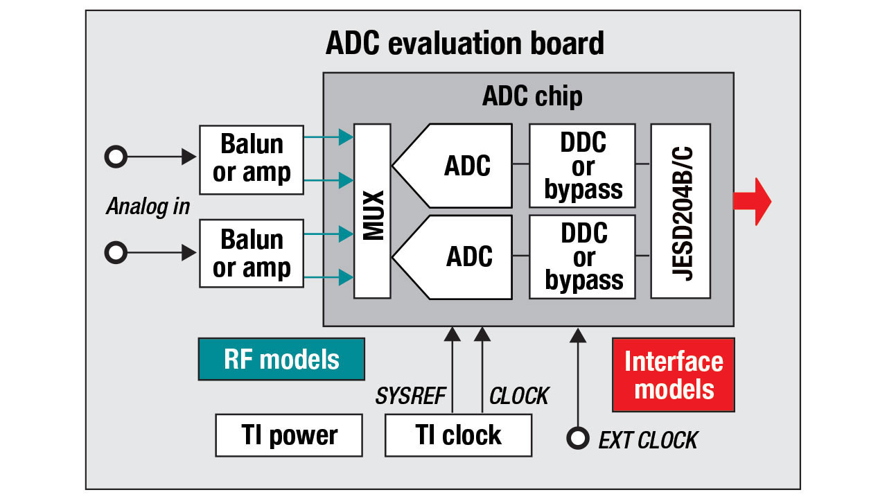 Figure 4 Modeling the interfaces
Conclusion
If it’s been a while since you’ve designed with high-speed data converters, or if you’re relatively new to high-speed design, you can take comfort in knowing that TI is making them easier to use. We’ve put together a complete development environment to make all of this easier, shown in Figure 5.
With ready-to-use IP for easy FPGA integration, precise RF system models, and the most robust set of flexible, scalable and automatable evaluation modules on the market, you can cut months of firmware development time, reduce costly design cycles and accelerate your high-speed design from concept to prototype.
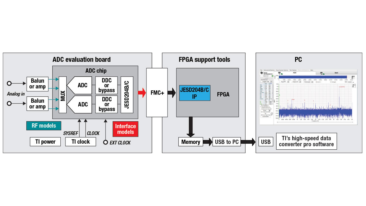 Figure 5 Typical high-speed analog-to-digital converter (ADC) evaluation environment
Additional resources
- Evaluate your high-speed data converter or AFE platform using our high-speed data converter pro software.
- Brush up on the basics in our TI Precision Labs training series, “High-Speed Analog-to-Digital Converter (ADC) Fundamentals.”
- Learn more about the differences between JESD204 standards in our application report, System Design Considerations when Upgrading from JESD204B to JESD204C.
- Learn more about S-parameter models in our technical article, “So, what are S-parameters anyway?”