SSZT360 november 2019 ADS7042 , ADS7138 , DAC43401 , DAC53401 , DAC53608
(Note: Kaustubh Gadgil and Robert Schreiber co-authored this technical article.)
With the increased trend toward smaller systems, every square millimeter of printed circuit board (PCB) area matters. At the same time, with the increased demand for data, more sensors need to be monitored.
In this article, we’ll discuss how you can significantly reduce PCB footprint, increase channel density, and leverage higher integration of other components and features with TI’s small data converters, providing more value in a smaller size.
Benefit No. 1: a smaller PCB footprint
With advancement in design and packaging technologies, electronic components have gotten smaller. As shown in Figure 1, TI’s latest single-channel ADC, ADS7042, is available in a 2.25-mm2 footprint, nearly half the size of comparable ADCs of a decade ago. Similarly, TI’s latest single-channel DAC, DAC53401, is one-fourth the size of comparable DACs of a decade ago. Likewise, for multi-channel applications, TI’s latest 8-channel ADC (ADS7138) and DAC (DAC53608), are both offered in a footprint of 9 mm2 (~1 mm2 per channel).
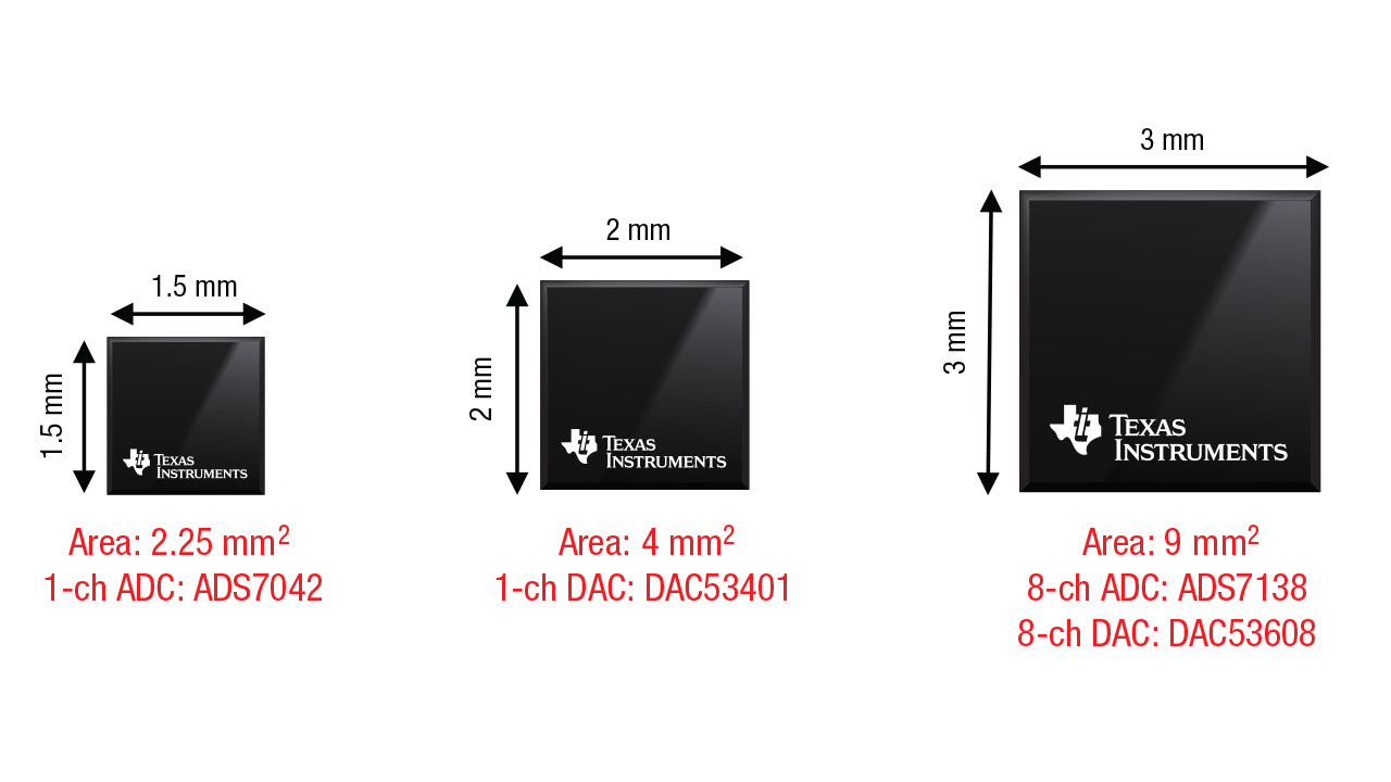 Figure 1 TI’s Smallest Data
Converters
Figure 1 TI’s Smallest Data
ConvertersThese tiny data converters allow you to reduce the PCB size for space-constrained designs or pack more channels into the same PCB size, or both.
Benefit No. 2: integration of analog functions
Many systems use discrete components and passives to implement a variety of analog functions, such as signal conditioning, biasing and comparators. Because TI’s smaller data converters integrate these functions, they eliminate many discrete and passive components, thereby reducing PCB size, simplifying design, improving performance and increasing reliability.
- Fewer external components As shown in Figure 2, DAC53401 integrates an output buffer as well as an internal reference, saving PCB area and cost.
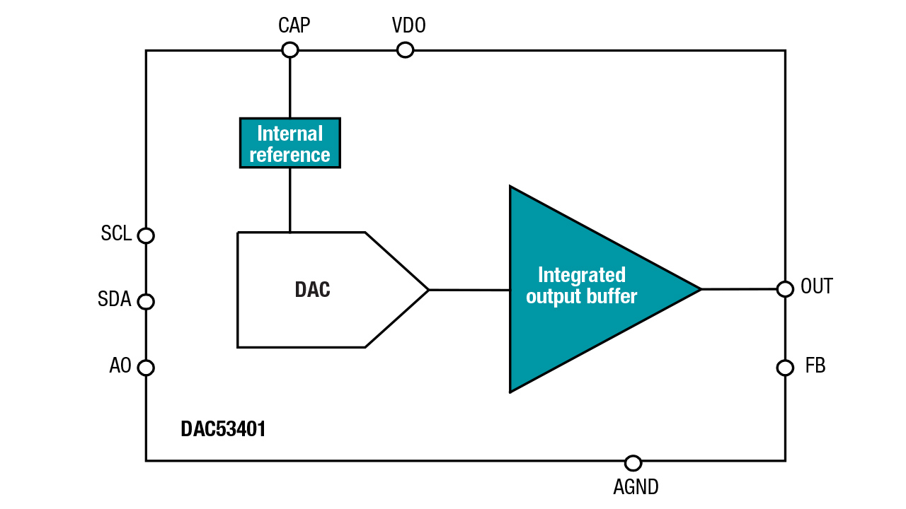 Figure 2 Integrated Reference and
Buffer in DAC53401
Figure 2 Integrated Reference and
Buffer in DAC53401Another example is the ADS7138 shown in Figure 3, which does not need a driver amplifier at the input for most applications, again saving PCB area and cost.
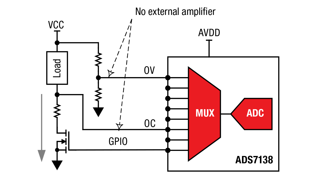 Figure 3 ADS7138 Eliminates the Need
for an External Amplifier
Figure 3 ADS7138 Eliminates the Need
for an External Amplifier- Bias
voltage generation, both fixed and variable The electrically erasable
programmable read-only memory (EEPROM) and slew-rate control features of the
DAC53401 are a good fit for generating fixed or variable bias voltages. Figure 4 shows an example of a lighting application.
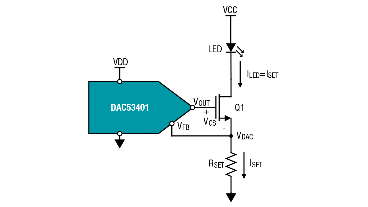 Figure 4 DAC53401 Biasing an
LED
 - Analog and digital
comparator Comparators are often used in systems to alert the host
controller immediately if any of the critical signals, such as currents,
voltages and temperatures, deviate outside their expected range. This comparator
should have fast response time and avoid false alarms.
As shown in Figure 5, the separate feedback pin (FB) enables you to use the DAC53401 as an analog comparator with a programmable threshold voltage.
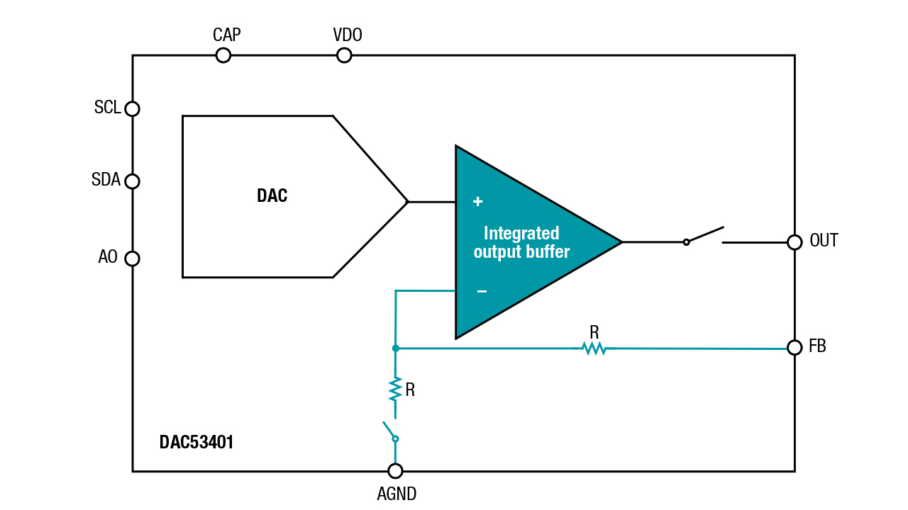 Figure 5 DAC53401 Offers Access to the
Feedback Path of Its Internal Amplifier
Figure 5 DAC53401 Offers Access to the
Feedback Path of Its Internal AmplifierAs shown in Figure 6, the ADS7138 integrates a digital comparator function with features such as programmable thresholds, hysteresis and event counter, which significantly reduce the possibility of getting a false alarm.
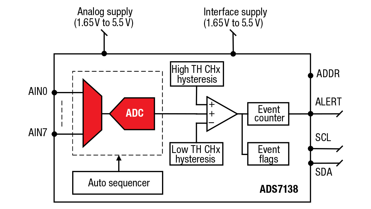 Figure 6 ADS7138 as a Digital
Comparator
Figure 6 ADS7138 as a Digital
ComparatorBenefit No. 3: integration of digital features
A smaller data converter not only enables remote sensor conditioning, it also enables remote data processing. Local processing improves the performance of the remote sensor, reduces the response time in the event of an alarm, and frees up some processing bandwidth in the central processor.
- Output averaging to improve
noise performance It is a common practice to average sensor readings
over a short period of time to reduce the effects of noise in the system. As
shown in Figure 7, the ADS7138 can average as many as 128 samples, reducing the effects of noise by over 10 times.
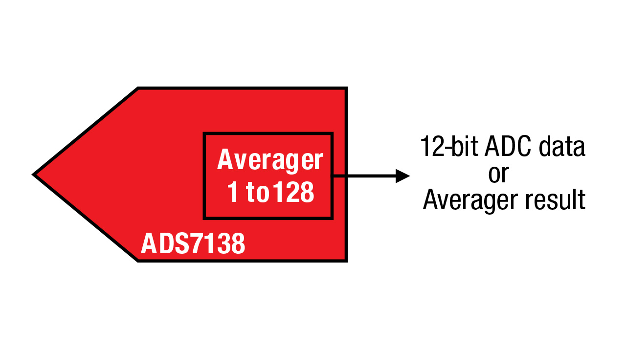 Figure 7 Averaging Feature
inside ADS7138
 - General purpose input/output (GPIO) In many systems, the detection
of an alarm event requires immediate control action (like switching off a
heating element or turning on a hazard indicator). In the ADS7138, some of the
analog input channels can monitor the sensors, while the unused analog input
channels can serve as GPIO pins. As shown in Figure 8, the monitored sensor can control the status of GPIO pins
locally, or a central processor using the I2C interface can control the status
remotely.
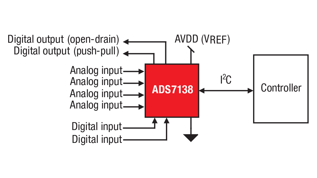 Figure 8 ADS7138 as Adc and
Gpio
 - Waveform generation In
some systems, you need to generate certain waveforms to produce tones (like in
medical applications) or create LED breathing effects (like in lighting
applications). DACs like the DAC53401 come with a feature called continuous
waveform generation, enabling you to generate triangle, square, trapezoidal or
sawtooth waves, as shown in Figure 9.
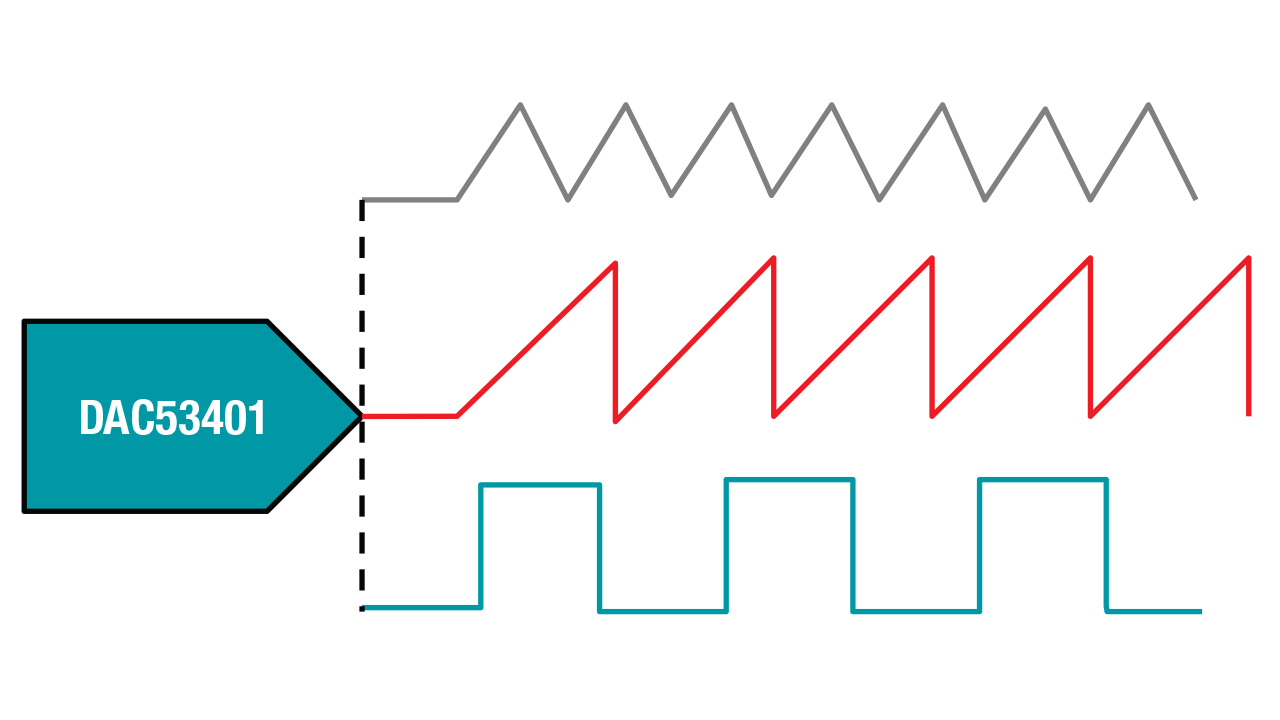 Figure 9 DAC53401 Generating
Multiple Waveforms
 - Cyclic redundancy check (CRC) When using ADCs such as the ADS7138 for critical monitoring functions or redundant measurements, it becomes imperative to maintain data integrity. As shown in Figure 10, the ADS7138 achieves this by implementing CRC on the data communication between the ADC and the central processor.
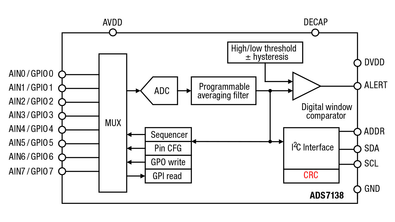 Figure 10 ADS7138 with CRC on Input and
Output Data
Figure 10 ADS7138 with CRC on Input and
Output DataAs shown in Figure 11, DACs like the DAC53401 and DAC43401 use CRC to make sure that whatever is written to or loaded from the nonvolatile memory or EEPROM is not corrupted.
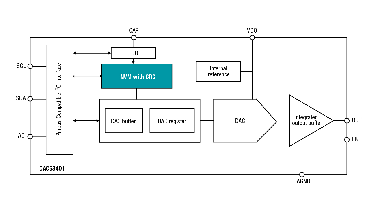 Figure 11 DAC53401 with Crc on
Nvm
Figure 11 DAC53401 with Crc on
NvmIntegrating these analog functions and digital features may lead to a more complex integrated circuit, but it can greatly reduce overall system complexity by adding processing and diagnostic capabilities.
Additional resources
- Explore the DAC53401 and DAC43401 data sheet.
- Learn how the DAC53401 and DAC43401 present a LED and laser diode biasing solution for commercial and automotive applications.
- Explore the ADS7138 data sheet.
- Learn how the ADS7138 can help reduce false triggers using digital comparator.