SSZT471 june 2019 CSD19536KTT , CSD87353Q5D
In power semiconductors, design engineers use the safe operating area (SOA) to determine whether it’s possible to safely operate a device such as a power metal-oxide semiconductor field-effect transistor (MOSFET), a diode or an insulated-gate bipolar transistor (IGBT) at current and voltage conditions in their application without causing damage to itself or nearby devices.
New integrated devices such as power blocks and power stages require a different way to specify SOA. As shown in Figure 1, a power block integrates control and synchronous FETs in a half-bridge configuration. A power stage adds a driver integrated circuit to the power block.
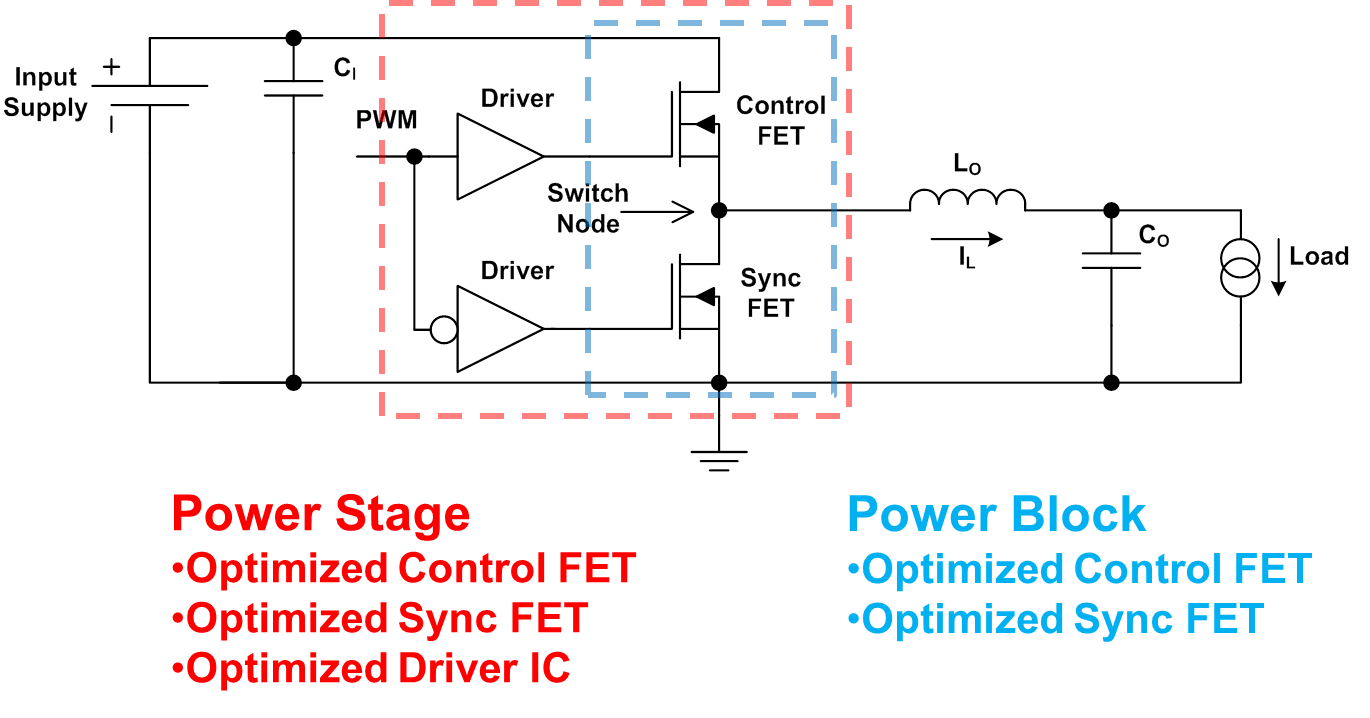 Figure 1 TI’s Definition of Power
Blocks and Power Stages
Figure 1 TI’s Definition of Power
Blocks and Power StagesA New Approach to an Old Problem
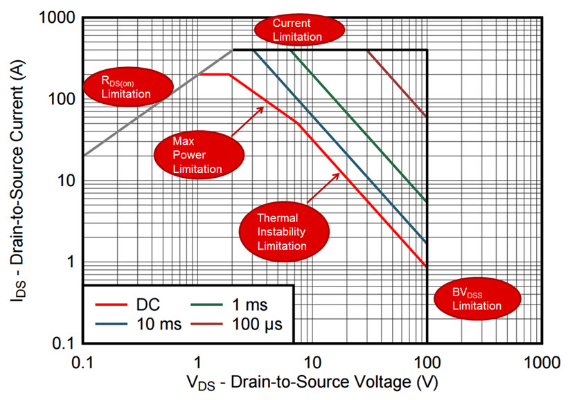 Figure 2 Datasheet SOA of the
CSD19536KTT Power MOSFET
Figure 2 Datasheet SOA of the
CSD19536KTT Power MOSFETUnlike discrete MOSFETs, which fit into a multitude of applications, power blocks are optimized for use in switch-mode applications such as power supplies and motor drives. As such, discrete FET SOA curves don’t work for power blocks. To help designers, TI provides SOA information for power blocks in a way that correlates with the intended application.
SOA curves in TI power block datasheets are derived from power loss and thermal data collected with the device operating in an application circuit, such as a synchronous buck converter. Power blocks optimized for motor-drive applications are tested in a half-bridge configuration at a 50% duty cycle with a fixed output inductor. The SOA curves plot output current vs. temperature (printed circuit board [PCB] or ambient) and provide guidance on the temperature boundaries within an operating system by incorporating both thermal resistance of the package and system power loss.
Power-supply manufacturers provide similar SOA and thermal derating curves for their products. TI is leveraging this approach because power blocks are normally used in switch-mode power supply and motor drive applications.
Understanding Power Block SOA
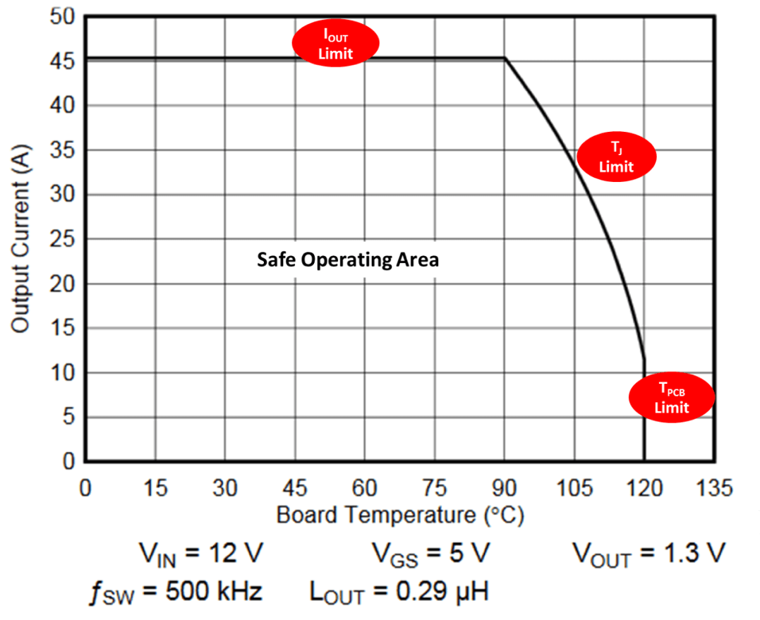 Figure 3 Typical Datasheet SOA for the
CSD87353Q5D Power Block
Figure 3 Typical Datasheet SOA for the
CSD87353Q5D Power BlockThe region below the curve is the SOA for the power block and is defined by three distinct boundaries:
- The horizontal line at the top of the graph is the maximum recommended output current for the application: 40 A.
- The curved boundary to the right is the maximum junction temperature limit.
- The vertical line on the lower right is the maximum PCB temperature limit – 120°C for most applications. This temperature may vary depending on the PCB material and your design specifications.
Figure 4 and Figure 5 show datasheet SOA curves for the CSD87353Q5D and display the power block output current vs. ambient temperature in vertical and horizontal board orientations, respectively, with varying airflow conditions.
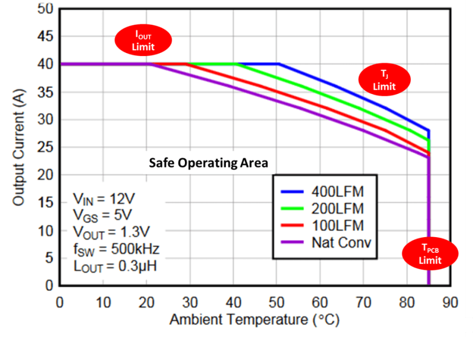 Figure 4 CSD87353Q5D Safe SOA – PCB
Vertical Mount
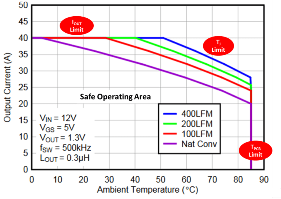 Figure 5 CSD87353Q5D SOA – PCB
Horizontal Mount
Figure 5 CSD87353Q5D SOA – PCB
Horizontal MountThese SOA plots are based on measurements made on a 4-by-3.5-by-0.062-inch PCB design and six copper layers with a 1-ounce copper thickness each. As shown in Figure 3, the region below the curves is the SOA, with boundaries defined by the recommended maximum output current, maximum junction temperature and maximum ambient temperature in the application. In this case, TI chose 85°C as the maximum ambient temperature, as most power block applications fall within this limit. Again, this temperature can vary based on your application and requirements.
In addition to the SOA curves, the power block datasheet includes plots of measured power loss and normalized graphs that allow you to calculate adjustments to the SOA for your specific design and operating conditions. Detailed instructions and design examples are included in the Application and Implementation section of the power block data sheet.
The SOA is critical when determining whether a power device can operate in your application without damaging itself or devices around it. TI provides SOA data for integrated power blocks based on power loss and thermal data tested in an application circuit, an approach that correlates with how the device is used in your design. TI leverages the industry-standard SOA and thermal derating approach used for many years by power-supply manufacturers allowing you to confidently design the power block into your application.
Additional Resources
- Visit us on ti.com: www.ti.com/mosfet
- Learn the basic tips and tricks to select and design with a MOSFET 101
- Read our MOSFET Blog Series
- Find out what a Lead Free MOSFET really means
- Read more about Motor Drives
- Use our Buck Converter FET Selection Tool