SSZT525 march 2019 DAC43608 , DAC53608
Many imaging products are moving toward more efficient LED array-based solutions and away from traditional technologies such as lasers or lamps. Applying resistive voltage dividers enables the linear forward biasing of LEDs for proper operation. However, because the biasing point of any LED can change across temperature – as well due to actual device-to-device variability – programmability of the particular biasing point then becomes a requirement in precision circuits.
Utilizing digital potentiometers (DPOTs), pulse-width modulation (PWM) or precision digital-to-analog converters (DACs) are common approaches for solving the biasing point programmability. But such solutions also need to be low-cost, small sized and include a high level of integration. Selecting the right architecture then becomes a nontrivial issue. In this blog post, I will discuss the different low-side LED biasing topology options and their respective trade-offs.
DPOT-based Biasing
LEDs are usually biased with current; Figure 1 illustrates the most basic implementation of a programmable current source using a typical DPOT with an adjustable shunt reference. Varying the voltage across the Zener changes this circuit’s current. While the Zener approach is effective, a major drawback is that it requires additional components that leads to an increased bill of materials (BOM), footprint and ultimately cost – which is especially pronounced when biasing an array of LEDs. Further, the base-to-emitter voltage (VBE) of the transistor can also vary with temperature and collector current, which can be further undesirable to the design.
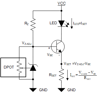 Figure 1 DPOT-based Biasing
PWM-based Biasing
It is also possible to use a PWM signal instead of a DPOT and Zener to program the bias point. In such cases, the bias point corresponds to the DC value of the PWM signal. While simple to implement, such a circuit also requires one PWM generator per channel, which may be difficult to support depending on what microcontroller you’re using (if any). Another consideration is that a continuous PWM also creates potential distortion and electromagnetic interference-related issues.
A Simple Biasing Method Using a Precision DAC
Another way to solve the biasing point programmability is to use a simple precision DAC to provide the biasing circuit. Figure 2 depicts this configuration, including the use of the 10-bit, 8-channel, buffered-voltage-output DAC53608. This approach provides a circuit with the smallest size and lowest BOM cost.
Keep in mind, however, that like the previous circuit, drift can exist within the VBE of the transistor, and the output may also require some headroom near the ground rail due to the expected VBE drop.
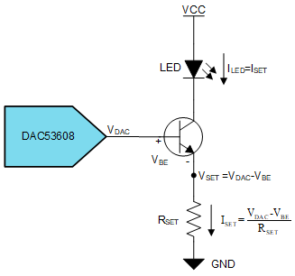 Figure 2 Programmable LED Biasing
Circuit
Figure 2 Programmable LED Biasing
CircuitWhile the VBE can vary with temperature and collector current, you can ignore such variations in applications that place the circuit inside a larger feedback loop with gain. With that said, there may be concern for applications that are open loop and that do not employ temperature calibration. The drift in VBE due to temperature and collector current can lead to gain error and full-scale error at the system level.
A robust way of compensating for such VBE variation is to place the circuit inside the feedback loop of an amplifier, as shown in Figure 3. This circuit is very suitable for applications that require high accuracy; the only drawback is the additional amplifier.
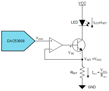 Figure 3 VBE Compensation
Using Buffer
Figure 3 VBE Compensation
Using BufferFigure 4 shows yet another approach for compensating VBE: using a matched pair of P-channel N-channel P-channel and N-channel P-channel N-channel transistors to cancel out the voltage variations and any headroom. As you can see, this circuit helps balance the benefits of accuracy, solution size and cost.
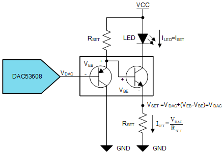 Figure 4 VBE Compensation
without Buffer
Figure 4 VBE Compensation
without BufferFigure 5 compares each topology. The precision DAC-based solution stands out over the other approaches in many aspects. General-purpose precision DACs in 8- and 10-bit resolutions have been flooding the market for a long time, but the DAC53608 (and its device family) provides the latest semiconductor technology to enable easily implemented, smaller, ultra-low-cost LED biasing solutions.
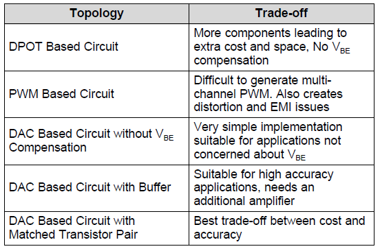 Figure 5 Comparison of LED Biasing Topologies
The DAC53608, first in a family of small DACs, is an eight-channel buffered-voltage-output DAC packaged in a tiny 3-mm-by-3-mm QFN package. It offers single-supply operation and also comes in an 8-bit pin-compatible version, the DAC43608. These DACs provide an I2C interface whose device address can be configured for up to four different values using a single hardware pin, which allows the use of as many as 32 channels without the need for an I2C buffer.
Could the DAC53608 be part of your LED-biasing circuit design?
