SSZT681 june 2018 DP83640 , LMK05028
As current telecommunication networks move from legacy synchronous optical networking (SONET)/synchronous digital hierarchy (SDH) networks to Ethernet transport networks, more and more services are concurrently becoming time critical.
For example, in financial markets, applying the Institute of Electrical and Electronic Engineers (IEEE) 1588 precision time protocol (PTP) achieves accurate timestamping in high-frequency trading. PTP is a protocol used to synchronize clocks throughout a network. It is independent of the physical layer to distribute time of the day and frequency, but it can be affected by impairments of the network such as packet delay variation.
Another standard for frequency synchronization is Synchronous Ethernet (SyncE), which transports accurate frequency information through the Ethernet physical layer (PHY). It uses the physical layer of Ethernet, and is not be affected by impairments introduced by the higher levels of the network. Combined with SyncE, IEEE1588 PTP can achieve better synchronization result than pure PTP without SyncE. Modern Ethernet switches can support both the SyncE and IEEE 1588 PTP to implement time (or phase) and frequency synchronization.
For example, TI’s LMK05028 network synchronizer clock integrates two independent PLL channels, (either channel can support SyncE clocks or IEEE1588 PTP slave clocks), This means that one unit LMK05028 can output SyncE domain clocks without PTP tuning and IEEE 1588 domain clocks with PTP tuning at the same time.
In this post, I’ll show you how to use the LMK05028 to implement an IEEE 1588 slave with SyncE.
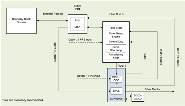
There are two phase-locked loop (PLL) channels in the LMK05028: one for the SyncE domain and the other for the IEEE 1588 domain. A field-programmable gate array (FPGA) or central processing unit (CPU) hosts the IEEE 1588 PTP stack, timestamp engine, time-of-day logic, servo software loop and anti-aliasing filter. The timestamp engine can recover a PTP clock from PTP packets on the Ethernet interface, or lock to an optional external 1PPS input from GPS via the LMK05028.
The LMK05028 generates synchronized system clocks to the FPGA or CPU, which then calculates the frequency and phase difference between the internal PTP clock and the feedback system clock. Based on the result, the FPGA or CPU will dynamically adjust the frequency in digitally controlled oscillator (DCO) mode using I2C/Serial Peripheral Interface or direct pin control via the FINC/FDEC pins. In this configuration, the LMK05028 output clocks always track the PTP correction word or GPS (1PPS). The ability to lock to a 1PPS input and generate a 1PPS output gives you additional flexibility in your applications. The LMK05028 can lock to 1PPS input directly without DCO tuning, which can help the FPGA or CPU release resources.
 Figure 1 The LMK05028 Working as a
Slave Clock.
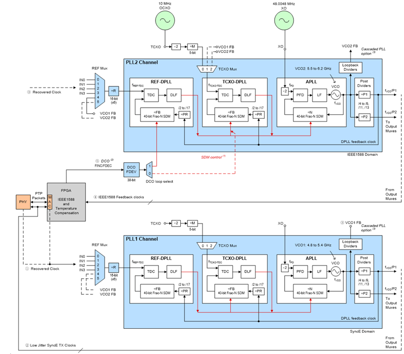
  Figure 2 LMK05028 Three-loop Mode for a
SyncE and IEEE 1588 Slave
Figure 2 LMK05028 Three-loop Mode for a
SyncE and IEEE 1588 SlaveThe LMK05028 has two PLL channels that integrate voltage-controlled oscillators (VCOs) covering different frequency ranges. VCO1 covers 4.8GHz to 5.4GHz and VCO2 covers 5.5GHz to 6.2GHz. You can operate the PLL1 channel’s VCO at 5GHz or 5.15625GHz to generate Ethernet clocks.
The PLL1 channel is dedicated to the SyncE domain. The basis of SyncE is that the transmitter clock should be synchronized with the receiver clock in frequency, so PLL1 gets a recovered clock from the PHY or FPGA as the reference.
The PLL1 channel outputs a low-jitter SyncE clock for transmitting the PHY and Media Access Control (MAC). The PLL2 channel can also select the noisy SyncE recovered clock as a reference through the internal REF multiplexer, which is the same as the PLL1 channel reference.
I recommend using the three-loop DCO mode on the PLL2 channel for IEEE 1588 clock adjustment. In this mode, either software or pins FINC and FDEC can control the fractional-N sigma-delta modulator (SDM) of the REF-DPLL module directly. Some output clocks from the PLL2 channel (for example, 1PPS, 10MHz or 125MHz) feed back to the internal timestamp engine of the FPGA.
This is how the LMK05028 network synchronizer clock implements an IEEE 1588 slave and SyncE with two PLL channels in different modes. TI has published the LMK05028’s test report compliance to the International Telecommunication Union (ITU)-T G.8262 standard.
With its novel three-loop architecture and other features - including hitless switching with phase cancellation 1PPS phase lock, zero delay mode and robust window detector - the LMK05028 is not limited to communications; it is also a good fit for industrial applications like smart grids, medical imaging and broadcast video.