SSZT688 june 2018 OPA2810
As an introduction to this post, let me provide some background. Voltage-feedback amplifiers are sometimes categorized based on the type of transistors in the device: either bipolar, complementary metal-oxide semiconductor (CMOS) or junction field-effect transistor (JFET). A few amplifiers may even use a combination of these transistors to extract their benefits in various amplifier stages. For example, JFET-input amplifiers include an input differential pair using JFETs which enable a very large amplifier input impedance, which is followed by gain and output stages using bipolar transistors.
JFET-input amplifiers are used as test and measurement analog front ends, current sense amplifiers, analog-to-digital converter (ADC) drivers, photodiode transimpedance amplifiers, or as a multichannel sensor interface through multiplexers. In this post, I’ll discuss the advantages of using JFET-input amplifiers in these applications using the OPA2810 as an example. The OPA2810 is a 110MHz, 27V, wide-input differential voltage (VIN,Diff) tolerant rail-to-rail input/output FET input amplifier.
Data Acquisition and Current Sensing
| Jump-start your high-speed application design | |
|
Quickly and easily demonstrate the functionality and versatility of the OPA2810 with the evaluation module. Learn more. |
Test and measurement equipment must also recreate input signals on the amplifier output accurately, which is enabled with the exceptional distortion performance of the OPA2810 due to its large 75mA linear output drive capability. Since the equipment usually is line-powered, the amplifier must operate off supply voltages greater than 24V.
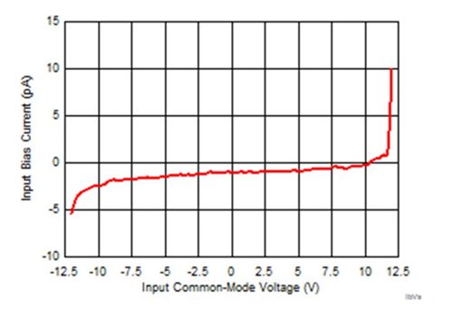 Figure 1 Bias Current Variation with
Input Common-mode Voltage for the OPA2810
Figure 1 Bias Current Variation with
Input Common-mode Voltage for the OPA2810Wideband Photodiode Transimpedance Applications
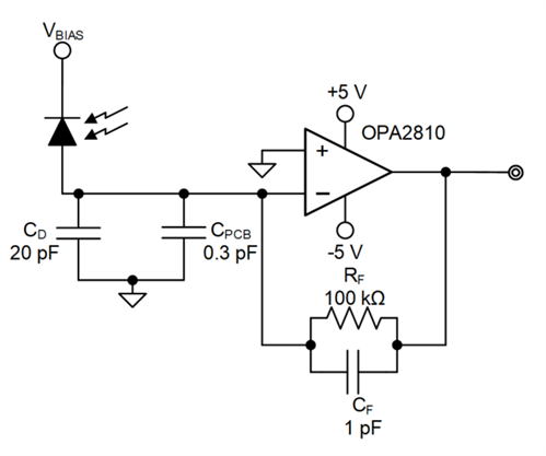 Figure 2 Photodiode Transimpedance Amplifier Circuit with Feedback Compensation Capacitance
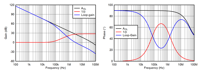 Figure 3 Gain Magnitude and Phase Bode Plots for the Transimpedance Amplifier in Figure 2
Multichannel-input Data-acquisition Systems
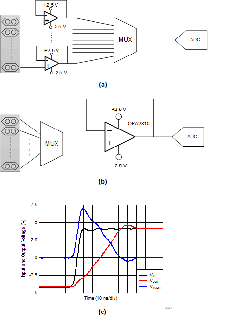 Figure 4 A Multichannel Sensor Front End with Multiple Slow-settling Amplifiers (a); Using a Single OPA2810 with Fast Settling (b); Large-signal Transient Response Using the OPA2810 (c)
Because of the fast input transient, the amplifier is slew-limited and the inputs cease to track each other (a maximum VIN,Diff of 7V is seen Figure 4c) until the output reaches its final value and the negative feedback loop is closed. For standard amplifiers with a 0.7-1.5V VIN,Diff rating, you must use current-limiting resistors in series with the input pins to protect from irreversible damage, which also limits the device frequency response. The OPA2810 has in-built input clamps that allow the application of as much as 7V of VIN,Diff, with no need for external resistors and no damage to the device or a shift in performance specifications. Such an input-stage architecture coupled, with its fast settling performance, makes the OPA2810 a good fit for multichannel sensor multiplexed systems.
ADC Drivers
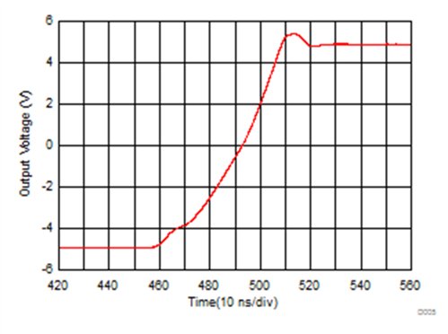 Figure 5 Large Signal Transient and Settling Response
Hence, JFET-input amplifiers, like the OPA2810, offer a variety of benefits in different high-speed applications discussed above due to their high-Z inputs, superior distortion performance, fast settling and wide-supply range. Make sure to look at the family of high-Z input high-speed amplifiers from TI to select the one that best suits your application requirements.
Additional Resources
- Download the Analog Design Journal article, “Source resistance and noise considerations in amplifiers” for more information on various amplifier topologies.
- Read the blog post, “What you need to know about transimpedance amplifiers – part 1.”
- Browse more than 40 training videos on operational amplifier (op amp) topics like noise, bandwidth and stability.
- Search TI high-speed op amps and find technical resources.