SSZT828 January 2018 TPS62088 , TPS62801 , TPS62823
Is it easy for you to physically see all of your integrated circuits (ICs) on your printed circuit boards (PCBs), or do you need a magnifying glass to see the small bits of black plastic sprinkled in among the larger resistors, capacitors and inductors? Over the previous few years, passive components – especially power inductors – have gotten smaller and smaller. 1608-sized inductors (1.6mm by 0.8mm) are now common, with rumors that 1005 sizes (1mm by 0.5mm) are coming soon.
These 0603 (60mils by 30mils) and 0402 (40mils by 20mils) sizes often made the ICs, at 2mm by 2mm or 3mm by 3mm, look large in comparison. Not anymore. For those of you designing the latest smartphones, personal electronic accessories and solid state drives (SSDs), the tables have turned. New solutions are available that are 80% smaller.
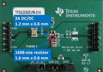
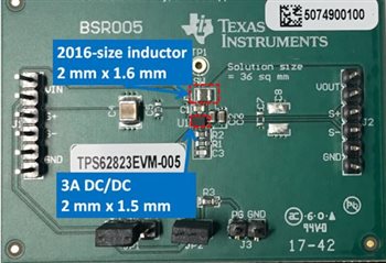
A 3A step-down (buck) converter (TI’s TPS62088) is achievable in a mere 1.2mm by 0.8mm wafer chip-scale package (WCSP), which is a type of ball-grid array (BGA) package. That’s less than 1mm2 of board space for the DC/DC IC. If that’s too small for you, there’s also a 3A step-down converter (the TPS62823) in a larger and more traditional quad flat no-lead (QFN) package, measuring just 2mm by 1.5mm. Both of these power-supply ICs are once again smaller than the power inductors surrounding them, as shown in Figure 1 and Figure 2.
 Figure 1 A 3A DC/DC Is Smaller than
a 1608-Size Resistor
 Figure 2 A 3A DC/DC Is Smaller than
a 2016-Size Inductor
Figure 2 A 3A DC/DC Is Smaller than
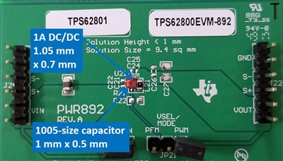
a 2016-Size InductorIs this still too big, you say? Although the above solutions are truly small for 3A devices, they offer much more power than what the smallest systems need, such as wearables. For these, 1A of output current is more than enough for any rail in the system. If you just need an amp or less, the TPS62801 shown in Figure 3 checks in at a mere 1.05mm by 0.7mm – not quite as small as a 1005-size component, but smaller than any 1A power supply on the market.
 Figure 3 A 1A DC/DC Is Almost as Small
as a 1005-Size Capacitor
Figure 3 A 1A DC/DC Is Almost as Small
as a 1005-Size CapacitorSo what’s the secret behind these smallest DC/DCs? Quite simply, a high switching frequency and a stellar silicon process. The three DC/DCs described here switch between 2.4MHz and 4MHz, which enables you to use either 0.24µH or 0.47µH inductors. With fewer physical turns of wire required on the inductor’s core to generate this very low inductance, physics says that it is easier to make the inductor smaller.
Of course, I can’t go into details as to what makes the power-optimized process so innovative; I’ll just let the results speak for themselves. The internal power transistors have both very low resistance and very low gate charge to produce high efficiencies at high currents, while switching at very high frequencies. Furthermore, the low quiescent current (IQ) of 5µA or less sustains the high efficiency down to very light loads.
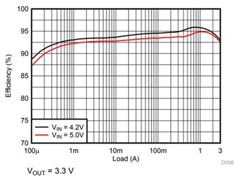
Figure 4 shows that the efficiency for a common 5VIN to 3.3VOUT converter is still very high at 93% even at its full 3A load, with a peak of 95% at a 1A load. Near 90% efficiency is maintained at a very light 100µA load. There is no efficiency degradation, even while operating at 4MHz. Such high efficiency results in longer battery life for portable systems and a lower temperature rise for both portable and stationary systems.
 Figure 4 TPS62088 Efficiency Is over
90% across the Entire Load Range
Figure 4 TPS62088 Efficiency Is over
90% across the Entire Load RangeIn your system, where do you need the smallest DC/DCs?
Additional Resources
- Read the article, "Choosing the optimal LPDDR4 power supply."
- Check out these blog posts:
- Order samples and evaluations modules (EVMs) for the TPS62088, TPS62823 and TPS62801.