SSZT873 November 2017 TPS61253A
1. Method to Prevent the Audible Noise Issue
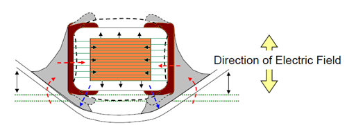 Figure 2 Mechanical Stress on the
Ceramic Capacitor
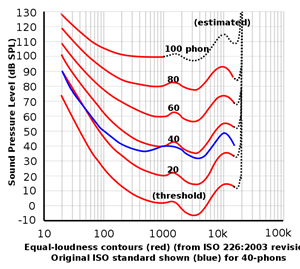
Equal-loudness contours (red) from ISO226:2003 revision, original ISO standard shown (blue) for 40-phons
Figure 3 Sound Pressure Level vs. FrequencyTo minimize the audible noise, both mechanical and electrical methods can be employed. The mechanical method is basically the PCB layout optimization but it can be a very difficult and complex task, and it can easily increase the manufacturing costs. The preferred method, which is electrical, can resolve the issue by means of controlling the circuit operation. One effective method is to employ a non-audible PFM scheme at light or no load condition. A good example is the TPS61253A boost converter, which includes a unique control technique to keep the PFM frequency above the audible band.
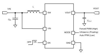 Figure 4 TPS61253A Typical Application Circuit
As shown in Figure 4, the TPS61253A can be configured by the MODE pin for different operation modes. There are three modes to choose from. When the MODE pin is pulled low, it operates in auto PFM mode. When it is pulled high, it is in the forced PWM mode. When it is left open or floating, it is set to the ultrasonic mode. These three modes can be selected dynamically during operation by externally reassigning the MODE pin condition.
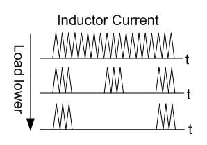
When the TPS61253A is configured in the ultrasonic mode, it automatically enters the PFM mode as soon as the valley current of the power inductor crosses zero. As the load decreases further, the valley current limit will go negative to reduce the number of skipped switching pulses, and this effectively prevents the subharmonic frequency from falling into the audible band. Bench tests prove that the subharmonic frequency in the ultrasonic mode is typically 53 kHz at no load condition, i.e. it will always stay above the audible band over the entire load range.
Figure 5 below shows the mode transition from PWM to PFM and then to ultrasonic mode with the load getting lighter and lighter.
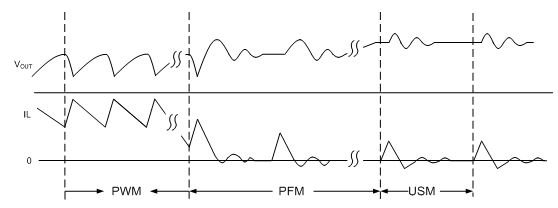 Figure 5 TPS61253A Operation Mode with Various Loads
Test Condition: VIN = 3.6 V, VOUT = 5 V, Load = 0 A, L = 0.56 µH, XEL3515-561MEB, COUT = 7 µF, Ultrasonic Mode
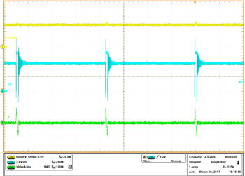 Figure 6 Steady State Waveforms of USM at No Load
2. Method to Cope with the RF Noise Issue
To avoid the potential noise interference with the NFC, the power converter should not generate noise in the sub-carrier frequency band. Otherwise, the application work-around solution like the PCB layout optimization or shielding must be implemented, and it undoubtedly raises the over cost.
Figure 7 shows the modulation scheme with subcarrier, with the subcarrier frequency varying from 12.7 MHz to 14.4 MHz.
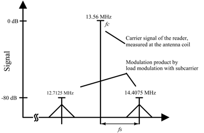 Figure 7 NFC Modulation Products Using Load Modulation with a Subcarrier
The proposed solution is to maintain the switching frequency of the boost converter above the subcarrier frequency band. This can be easily achieved with the TPS61253A. Its switching frequency can be conveniently set at 3.8MHz typical, always higher than the subcarrier frequency band, by configuring the MODE pin to the forced PWM mode.
Because the TPS61253A supports dynamic MODE programming during operation, it offers a valuable flexibility and programmability for a boost converter for different application environment. Figure 7 shows the efficiency of a typical design in different operation modes, including the Ultrasonic or Force PWM for low noise purpose, and the Auto PFM Mode for enhanced light load efficiency.
TPS61253A efficiency measurement is conducted at the conditions of:
VOUT = 5 V, Load = 100 µA – 200 mA, L = 0.56 µH, XEL3515-561MEB, COUT = 7 µF (effective@5V)
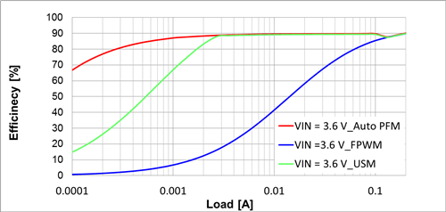 Figure 8 TPS61253A Efficiency at Auto PFM / Forced PWM / USM