SSZT910 october 2017 DAC38RF80 , TPS63710 , TPS7A8300
Do you need a negative voltage to power your data converter or amplifier? These types of systems usually require low noise to power such sensitive analog circuitry. While a linear regulator (LDO) is frequently used to achieve low noise, what if the switching DC/DC converter could provide low noise by itself? If you could use only a DC/DC converter, you could save significant bill of materials (BOM) costs, reduce your printed circuit board (PCB) space and remove additional power loss from your system.
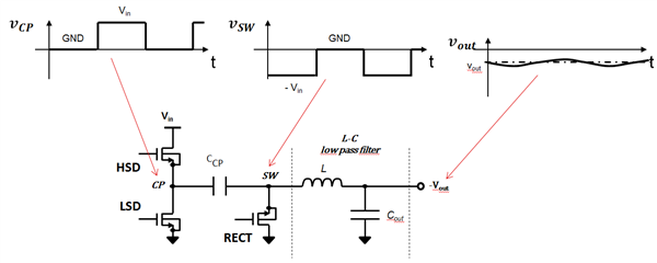
How does a low-noise inverting buck converter work? Figure 1 shows the basic schematic and typical waveforms from the TPS63710. The CCP capacitor, between the CP and SW pins, inverts the supply voltage, which is then further downregulated. The low-side (LSD) and rectifying (RECT) MOSFETs provide synchronous rectification for high efficiency. To begin a switching cycle, the high-side (HSD) and RECT MOSFETs turn on to charge CCP to VIN. Once charged, both the HSD and RECT MOSFETs open and the LSD MOSFET closes to deliver CCP’s stored energy to the output. The duty cycle is regulated to provide a low-noise and regulated output voltage.
 Figure 1 Simplified Schematic of a
Low-noise Inverting Buck Converter, TPS63710
Figure 1 Simplified Schematic of a
Low-noise Inverting Buck Converter, TPS63710The low-noise inverting buck converter is a voltage inverter – it creates a negative voltage. Because it is an inverting buck converter and not an inverting buck-boost converter, the output voltage (in absolute value) must always be below the input voltage for proper regulation.
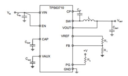
Let’s see how the entire solution benefits from the combination of all of its traits. Figure 2 shows the full schematic of the TPS63710 low-noise inverting buck converter.
 Figure 2 The Low-noise Inverting Buck
Converter TPS63710
Figure 2 The Low-noise Inverting Buck
Converter TPS63710Low noise is the most important characteristic when trying to achieve critical system performance parameters such as signal resolution and noise floor. The power supply, whether a switching DC/DC converter or otherwise, should not add additional noise to the system, because this noise can show up on the measured signal and result in distortions. The topology continuous output current and the device’s CAP pin enable the TPS63710 to achieve very low noise.
Continuous output current refers to the inductor being in series with the output stage and load. This is the same as in a typical step-down (buck) converter and supports a low output-voltage ripple from the switching action. Specifically, this topology keeps the output voltage free from most high-frequency noise that would otherwise be created by having a discontinuous output current across the output capacitor’s equivalent series resistance (ESR) and equivalent series inductance (ESL), as found in the traditional inverting buck-boost topology. While some high-frequency noise above 100MHz still couples through the inductor’s windings, you can easily filter this noise with a ferrite bead. The inverting buck topology creates a lower magnitude of switching ripple at its 1.5MHz switching frequency than the inverting buck-boost topology with the same output filter.
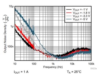
Additionally, the CAP pin reduces the self-generated, low-frequency 1/f noise, which typically comes from the voltage reference (bandgap voltage) inside the DC/DC. The external capacitor (CCAP) forms a low-pass filter with an internal resistor to achieve extremely small low-frequency noise below 100kHz, as shown in Figure 3. This noise-reduction functionality is the same as what’s found on a high-performance LDO’s noise reduction and soft-start (NR/SS) pin, such as in the TPS7A8300, and is the biggest concern in many telecommunications systems since this noise occurs within the bandwidth of the transmission channel and is difficult to filter out. Including this 1/f-noise filter inside the DC/DC reduces the low-frequency 1/f noise to acceptable levels.
 Figure 3 Output Noise Density of a
Low-noise Inverting Buck Converter
Figure 3 Output Noise Density of a
Low-noise Inverting Buck ConverterAt last, there is a switching DC/DC converter with low noise to create that cumbersome negative rail in a single inverting step. Which part of your analog signal chain will it power?
Additional Resources
- Read the blog post, “Low-noise charge pumps make it easy to create negative voltages.”
- Check out the 3- to 11.5VIN, -5VOUT, 1.5A Inverting Power Module Reference Design for Small, Low-Noise Systems and 3V to 15.2V Input, 2A, -1.8V Inverting Power Module Reference Design for Up to 125°C.
- Order the DAC38RF80 dual-channel, 14-bit, 9GSPS, 6x-24x interpolating, 6 and 9GHz PLL DAC evaluation module.