SSZTAF6 february 2017 CSD86360Q5D , CSD87335Q3D , CSD87355Q5D
Many of today’s space-constrained designs use point-of-load (POL) converters with integrated power MOSFETs (iFETs) to solve engineering challenges. iFET converters offer integration that results in smaller space and ease of use. While these advantages are compelling, engineers often need a controller with specific features or functionalities that are not available in an iFET converter. Discrete MOSFETs or power blocks offer flexibility in meeting design targets in terms of efficiency, thermal performance and cost.
If you want to use an iFET converter, the desired control topology or required set of features such as PMBus interface, sync function or margining may not be available. In specific applications like battery charging, wireless charging, buck-boost circuits, multioutput converters or power-management integrated circuits (PMICs), an iFET converter may not even be an available option.
Discrete MOSFETs and power blocks allow you to tune the solution to your needs. Select these MOSFETs based on operating voltage, continuous current ratings, duty cycle and thermal environment. Using discrete components allows you to optimize performance and cost for the design at hand, albeit in a much larger footprint. Because a power block is a half bridge in a package, it offers advantages in terms of power density and simplicity of design – like iFETs – while maintaining application flexibility. TI offers 14 different footprint-compatible power blocks in two package types (3mm-by-3mm or 5mm-by-6mm small outline no-lead [SON]) optimized for different currents and duty cycles.
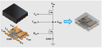
TI power blocks use PowerStack™ packaging technology (see Figure 1). This packaging technology eliminates parasitic elements between MOSFETs, resulting in higher efficiency and enabling higher frequencies while saving valuable board space versus discrete MOSFETs. The power block’s large grounded lead frame achieves excellent thermal performance compared to dual MOSFETs, which place the two devices side by side in a single package. You can place copper under the power block’s lead frame and use multiple vias to connect other ground layers in the printed circuit board (PCB) to pull heat from the package.
 Figure 1 TI Power Block Featuring PowerStack Packaging Technology
The PowerStack packaging approach, along with the large grounded lead frame, enables power blocks to achieve rated currents up to 25A in a 3mm-by-3mm package and 50A in a 5mm-by-6mm package with both high and low duty-cycle options. This means that you can still achieve small board space and use MOSFETs optimized for the specific application. Once you’ve selected a controller, you can find the right power block easily using the TI FET Power Loss Calculator.
Additional Resources
- Get more information about TI’s CSD87355Q5D, CSD86360Q5D and CSD87335Q3D NexFET™ power block products.
- Read the application report, “Power Loss Calculation with Common Source Inductance Consideration for Synchronous Buck Converters.”
- Read the white paper, “3-D packaging advancements drive performance, power and density in power devices.”