SSZTB37 July 2016 ADC32RF45 , LMX2582
What is all the fuss about noise? Engineers are generally aware of noise in electrical circuits. Interestingly, each engineering discipline tends to characterize noise differently:
- Analog engineers typically characterize noise with a normalized noise voltage determined by calculating the nanovolts per root hertz (nV/sqrt(Hz)).
- Data converter engineers tend to specify the signal-to-noise ratio (SNR). SNR references signal power to overall noise power within the Nyquist zone.
- Radio-frequency (RF) engineers work with the device noise figure (NF). Noise figure represents the incremental noise that a circuit block adds to the system. In communication applications, noise is a critical component to meet system requirements.
The RF sampling architecture changes the landscape of receiver analysis. The RF sampling analog-to-digital converter (ADC) is a key block in the receiver lineup. The RF sampling converter combines the analysis of data converters with traditional RF lineups. Cascade analysis operates with NF and gain parameters to translate individual block characteristics to a system noise figure. In turn, the system noise figure determines the receiver sensitivity. Sensitivity is the lowest signal power that is properly demodulated. With RF sampling ADCs, you must convert the measured SNR parameters to a noise figure parameter for proper cascade analysis.
SNR specifications are not necessarily as straightforward as they first appear. SNR data found in a device’s data sheet is usually measured with the desired signal near full scale. That situation is valid when a large blocker or interference signal is in the band; however, it is not applicable when measuring small signals. The noise performance of the RF sampling ADC varies depending on the input signal. For a pure sensitivity measurement, noise spectral density (NSD) is the optimum parameter. NSD measures the entire noise power in the converter’s Nyquist zone divided by the Nyquist bandwidth. Equation Figure 1 shows the calculated NSD as a function of measured SNR performance at a given input power and the device’s full-scale voltage, input impedance and sampling rate:
 Figure 1 (1)
The formula may seem daunting, but most of the parameters are fixed for a given device. The full-scale ADC voltage and input impedance are fixed. You specify the sampling rate up to the device’s maximum. The SNR performance for a given device is ideally fixed, but there are some differences depending on input drive level and clock phase noise. Equation Figure 1 calculates the noise figure from the NSD referenced to the normalized thermal noise floor:
 Figure 2 (2)
The ADC SNR characterization typically uses an input signal near full scale. Under this circumstance, the sampling clock jitter and device’s aperture jitter contribute to overall SNR performance. For scenarios where the input signal is large, like in a jammer or blocking situation, this is a valid mode with which to characterize the device. In a pure sensitivity analysis, the input signal to the ADC will be low. SNR performance improves as the jitter contribution drops below the device’s thermal noise floor.
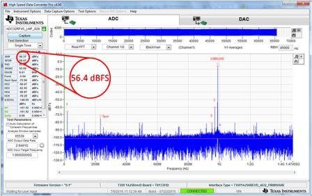
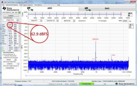
Look at the ADC32RF45 RF sampling ADC as an example. The full-scale voltage of the ADC is 1.35Vpp and the input impedance is 50Ω differential. The sampling rate is set near the maximum at 2,949.12MSPS. The LMX2582 provides a low-phase-noise clock signal. Figure 3a shows the spectrum and SNR performance with an input signal at 1,960MHz at 3dB below full scale. Figure 3b shows the same device under the same configuration, but with an input signal backed off by 40dB. The SNR performance improved by a factor of 6.5dB.

(a)

(b)
Figure 3 ADC32RF45 Large (a) and Small (b) Signal SNR PerformanceIn the small signal example the noise figure of the ADC is 26dB, as calculated by Equations Figure 1 and Figure 1. The NF value may seem high, especially compared to other typical devices in a receiver lineup. Most RF amps, filters or mixers are under 10dB NF. This value is rather typical for ADCs in general. Previous architectures often neglected the ADC noise figure because there was so much takeover gain in front of it. In the RF sampling architecture, there is only a low-noise amplifier (LNA) and variable gain amplifier (VGA) in front to provide the takeover gain. The NF performance of the ADC becomes a more significant contributor.
Figure 4 shows a simple lineup analysis. With reasonable levels for the LNA and VGA gain, the cascaded noise figure of the RF sampling lineup achieves a system noise figure less than 2dB. The analysis shows that the RF sampling architecture meets the most stringent sensitivity targets for communication systems with the proper selection of LNA. The RF sampling ADC eliminates the mixer and intermediate frequency (IF) amplifiers in a heterodyne architecture without negatively impacting overall sensitivity performance.
 Figure 4 Example Noise Figure Cascade
Analysis
Figure 4 Example Noise Figure Cascade
AnalysisCheck back next month when I will discuss an opposing situation: when the RF sampling receiver faces large input signals. You can also subscribe to Analog Wire to receive alerts when new blog posts are uploaded. Just click the subscribe button and log in!
Additional Resources
- Visit the High Speed Signal Chain University to watch the RF sampling video series.
- Read the white paper, “ Direct RF conversion: From vision to reality.”
- Search for solutions, ask questions and solve problems in the TI E2E™ Community High Speed Data Converter forum.
- Visit TI’s RF sampling page for a full suite of support resources, including TI Designs reference designs and application notes.
- See other posts in Russell’s RF sampling blog series.
- Learn about TI’s data converter portfolio and find technical resources.