SSZTB64 June 2016 ADC32RF45
** This is the 12th post in an Analog Wire RF sampling blog series . **
Radio frequency (RF) sampling receivers capture large signal bandwidths; in fact, I discussed how RF sampling analog-to-digital converters (ADCs) can capture 1GHz signal bandwidths in my previous post.
Capturing large bandwidths is great if you have them, but what about when your signals are not that wide? Automatically capturing such a large amount of bandwidth requires fast digital data rates, which strain the capabilities of the digital processor or field programmable gate array (FPGA). In addition, you may have a situation where your desired signals are separated in frequency space with unwanted signals or interference in other parts of the spectrum. You actually may not want to capture the entire spectrum, because then you have to deal with all the unwanted signals. You can alleviate this issue by using an RF sampling data converter that integrates digital-down converters (DDCs) and decimation filters.
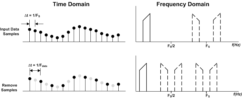
Decimation is a signal-processing technique primarily designed to reduce the data rate without impacting the signal. Decimation reduces the data rate simply by removing samples from the data stream. Figure 1 shows the time domain and frequency domain of a decimate-by-two operation, which eliminates every other sample. The integrity of the signal is not affected; however, the maximum signal bandwidth capability decreases. The decimate-by-two function is equivalent to a data converter clocked at half the original rate, with an analog anti-aliasing filter at half the original Nyquist bandwidth. The decimation filter eliminates unwanted signal images. It also eliminates half of the noise power. Since the desired signal remains unchanged and the noise power reduces by half, there is an overall signal-to-noise ratio (SNR) improvement. For a decimate-by-two operation, you will ideally get a 3dB SNR improvement. For any arbitrary decimation factor D, SNR improves by 20*log(D). The SNR improvement is not for free, however. You must sacrifice total bandwidth capability by a factor of Fs/2D, where Fs is the ADC’s sample frequency.
 Figure 1 Time and Frequency View of
Decimation
Figure 1 Time and Frequency View of
DecimationThe decimation filter works with digital mixers. The digital mixer converts the RF signal down to digital baseband. Decimation and filtering operate around the carrier located at baseband. The RF frequency signal is large, so the system requires a large sampling clock to properly capture the signal. The decimated signal at baseband generally has a relatively small maximum bandwidth. This reduces the data-rate requirement. Adhere to this rule of thumb: set the output sampling clock to meet your frequency planning guidelines and set your decimation rate to adequately capture the maximum signal bandwidth.
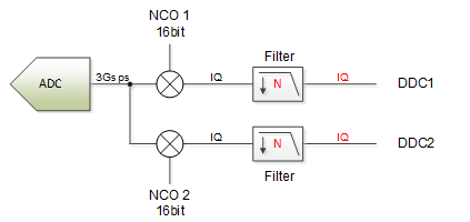
The DDC incorporates the mixer and decimation function. A numerically controlled oscillator (NCO) provides the mixer’s local oscillator (LO) frequency. A single DDC generally captures a single frequency band. But what if you need to capture multiple bands? Additional DDCs are the answer. Figure 2 illustrates an RF sampling ADC with two DDCs.
 Figure 2 Dual-DDC Block Diagram
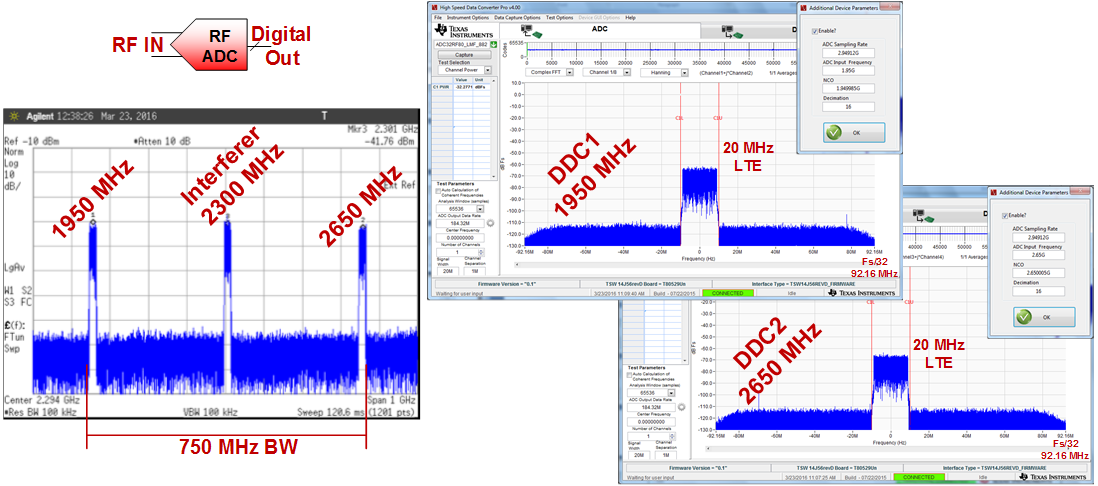
An RF sampling ADC with multiple DDCs provides powerful signal-processing capabilities. One application is for multimode, where the ADC captures two different bands while simultaneously filtering out unwanted bands or interference. Figure 3 shows a 20MHz Long Term Evolution (LTE) carrier located at 1,950MHz and 2,650MHz. There is also a third carrier located at 2,300MHz. With a straight RF sampling ADC operating at 3GSPS, the second Nyquist zone of the converter captures all three signals. The digital processor must account for the filtering of the unwanted carrier at 2,300-MHz. Further, transferring the full 1.5GHz of spectrum (one Nyquist zone) puts an undue burden on the processor or FPGA, since the bandwidth of any one carrier is relatively low.
A better approach uses an ADC with built-in DDC functionality like the ADC32RF45. The ADC32RF45 is a dual-channel, 14-bit, 3GSPS ADC. It includes two independent DDCs per channel. In this example, the ADC sets one NCO to the carrier at 1,950MHz and the other NCO to the carrier at 2,600MHz. The decimation factor is set to 16, which supports a maximum signal bandwidth of 187.5MHz. This is more than adequate to capture the 20MHz LTE carrier. The device captures each carrier and outputs it on an independent data stream. The DDCs effectively filter out the unwanted carrier at 2.3GHz.
 Figure 3 Dual-band Input Signal with
Interference and DDC Output for Each Band
Figure 3 Dual-band Input Signal with
Interference and DDC Output for Each BandNext-generation communication systems need flexible receiver solutions to meet customer requirements. RF sampling ADCs provide one level of simplification by capturing signals directly in the RF realm without the need for an analog mixer and analog LO synthesizer. An RF sampling converter that uses multiple DDCs provides additional integration. With a dual DDC operating in multimode, the ADC takes the place of two full channels. This gives you immediate space, cost and power savings. A simplified, lower-power receiver architecture opens the door for compact designs needed in large antenna arrays or massive multiple-in, multiple-out (MIMO) telecommunication applications. Take your designs to a lower cost and higher level with the next generation of RF sampling ADCs.
Check back next month, I will clarify all the fuss related to noise in RF sampling data converters. You can also subscribe to Analog Wire below to be alerted when all Analog Wire blog posts are live.
Additional Resources
- Visit the High Speed Signal Chain University to watch the RF sampling video series.
- Search for solutions, ask questions and solve problems in the TI E2E™ Community High Speed Data Converter forum.
- Visit TI’s RF sampling page for a full suite of support resources, including TI Designs reference designs and application notes.
- See other posts in Russell’s RF sampling blog series.
- Learn about TI’s data converter portfolio and find technical resources.