SSZTBF1 april 2016 LM22670 , LM22674 , LM22675 , LM22677 , LM22680 , LM25575 , LM25576 , LM2574 , LM2586 , LM2673 , LM2678 , LM2679 , LM2841 , LM2842 , LM2842-Q1 , LMR10510 , LMR12010 , LMR12020 , LMR14203 , LMR14206 , LMR62421
With the variety of regulators on the market, it can be difficult to choose a DC/DC regulator. Most automotive applications require high efficiency over the entire load range since they’re running from the battery. But then again, many industrial applications require good efficiency at high loads and efficiency at light loads is not very important. Understanding the losses in a DC/DC regulator is therefore important. Reading the efficiency curves in DC/DC converter data sheets also generates a few questions, such as “Why is the efficiency at light loads low?” and “Why does the efficiency dip at heavy loads?” In this blog series, I will attempt to deconstruct system efficiency into different component losses using the SIMPLE SWITCHER® LM2673 3A step-down voltage regulator as an example.
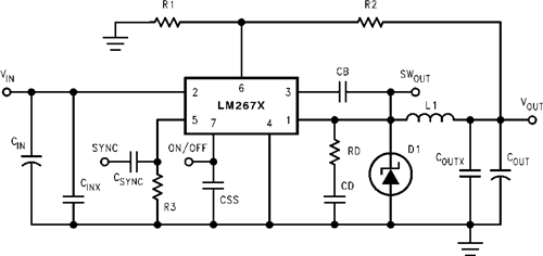
Figure 1 shows the evaluation module (EVM) schematic.
 Figure 1 Design Schematic
Gate Charge and IC Losses
In a typical nonsynchronous buck regulator such as the LM2673, the power-dissipating components are the IC itself, the inductor and the catch diode. The root-mean-square (RMS) currents through the input and output capacitors and the parasitic equivalent series resistance (ESR) are very low; thus you can ignore the losses in those components.
Due to their construction, every MOSFET has some parasitic capacitance between its terminals. They are the gate-drain capacitance (CGD), gate-to-source capacitance (CGS) and drain capacitance (CDS), as shown in Figure 1. The capacitance values differ based on MOSFET size, fabrication and other process parameters. Unlike in an ideal MOSFET – where there are zero transition times – the presence of these parasitic capacitances introduces finite switching times, as shown in Figure 2.
 Figure 2 MOSFET Parasitic Capacitances
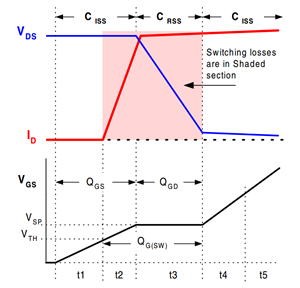
The finite switching times, as shown in Figure 3, are a result of the charging and discharging of the input capacitance (CISS). The input capacitance is basically the addition of CGS and the Miller capacitance (CGD). The gate charge (QG) is the addition of the gate-to-source charge (QGS) and the gate-drain charge (QGD). The gate charge of the MOSFET is the charge needed to completely turn the MOSFET on.
 Figure 3 Gate Charge and Miller Plateau
The MOSFET drivers provide the current (ICC) which you can estimate using Equation 1:
Where, FSW is the switching frequency of the DC/DC regulator.
For a converter like the LM2673, which has an integrated high-side MOSFET, the data sheet doesn’t list parameters like QG. Therefore, you’ll need to estimate the ICC in a different way: on the lab bench. With the device enabled and the load disconnected, measure the input current. Without a connected load, this input current measurement is essentially the ICC current measurement. The current ICC is also called the operating quiescent current. Please refer to the link in the ‘Additional Resources’ section to learn more.
For more accurate calculations, you can use TI’s WEBENCH® Power Designer software. WEBENCH Power Designer has information on all internal MOSFET parameters and therefore can take those into consideration while calculating losses.
As you can see from Equation 1, the current is directly proportional to the switching frequency (FSW). Since the MOSFET driver is providing this current, there are losses in the driver. The driver voltage (VCC) is set by the internal low-dropout regulator (LDO). The losses in the driver are expressed as shown in Equation 2:
Since the LDO internal to the DC/DC regulator provides this current, there will be power dissipation in the LDO as well. This power dissipation is expressed as Equation 3:
If you add up Equations Equation 2 and Equation 3, you’ll get the total power dissipation of the LDO and the driver (Equation 4):
Therefore, with higher input voltages, the loss increases. Also, the gate charge directly affects the switching losses. If the internal MOSFET has larger parasitic capacitances, then the resulting gate charge will be larger; the time spent in the switch transition will also be a bit longer. This will consequently increase the switching losses.
In the next installment of this series, I’ll explain how the gate charge is related to the switching losses in the MOSFET, how the light load efficiency is dependent on these losses, and how the total losses affect the conduction losses and overall efficiency of a DC/DC regulator.
Additional Resources
- The current ICC is also called the operating quiescent current. Read “DC/DC converter datasheets - Quiescent current” to learn more.
- Start a design now with WEBENCH Power Designer.
- Get more information on TI’s extensive portfolio of SIMPLE SWITCHER DC/DC regulators.