SSZTBN2 February 2016 SN65HVD72 , SN65HVD78
The last post in this series described the structure and basic operation of the RS-485 driver. In this post, I’ll discuss the RS-485 receiver and the relevant parameters in the RS-485 standard.
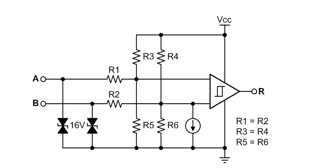
RS-485 transceivers such as the SN65HVD7x half-duplex family have an equivalent receiver input schematic like the one shown in Figure 1. 1) The receiver input circuitry consists of electro-static discharge (ESD) protection, a resistor-divider network, and a biasing current, all of which play a role in shaping the magnitude and common mode voltage that reaches the differential comparator.
 Figure 1 Differential Receiver Input
Structure
Figure 1 Differential Receiver Input
StructureESD Protection
The most important thing to note in terms of ESD protection for half-duplex transceivers is that the driver and receiver share the same ESD protection, saving space. But for a full-duplex transceiver, both the driver (Y and Z pins) and receiver (A and B pins) need independent ESD protection. This means you’ll need twice the area to support ESD protection.
Resistor-divider Network
The resistor-divider network on the A and B inputs serves two functions. The first function is to attenuate large signals that are beyond the range of the receiver’s supply voltage. This attenuation factor is necessary because the RS-485 standard states that voltages as low as -7V and as high as +12V can exist on the bus terminals to account for ground-potential differences that may exist between transceivers on a shared network. These high voltages need attenuation down to voltages that 3.3V or 5V transceivers can handle. A typical attenuation factor is on the order of 10-to-1, greatly reducing the magnitude of the voltages seen internally at the comparator.
The second important function of the resistor-divider network is to bias the bus voltages toward VCC/2. This is necessary because simply attenuating a negative signal will not bring the voltage between the receiver’s local ground and VCC. Attenuating the signal and biasing it toward VCC/2 prevents the inputs of the comparator from getting saturated; thus enabling the comparator to properly evaluate the differential voltage between the A and B terminals.
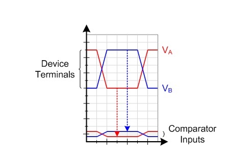
This ability to bias the voltages also allows the system to perform without a common ground connection between the remote RS-485 driver’s ground and the local RS-485 receiver’s ground. Figure 2 shows how an input signal is both attenuated and biased from the bus terminals to the input of the comparator through the resistor-divider network.
 Figure 2 Receiver Input-voltage
Attenuation
Figure 2 Receiver Input-voltage
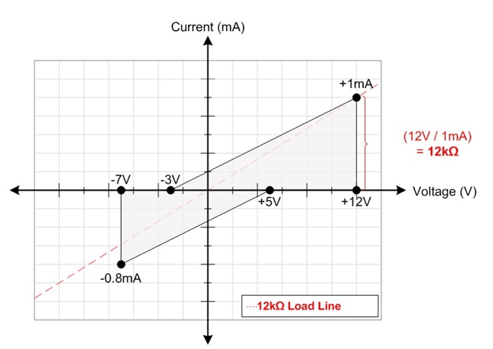
AttenuationThe series combination of R1 and R3 || R5 (resistors R3 and R5 in parallel) is the primary factor that determines the receiver’s input impedance. The RS-485 standard specifies that the input leakage current of a compliant receiver must remain within the shaded region shown in Figure 3 when applying -7V to +12V to the input terminals for both powered and unpowered conditions.
 Figure 3 RS-485 Receiver Input I-V
Characteristic
Figure 3 RS-485 Receiver Input I-V
CharacteristicThe trade-off that exists with receiver attenuator design is that in order to lower the leakage current, higher resistor values must be used, which increases the size of the resistors in the attenuator. Larger-sized components create a more expensive die and more parasitic capacitance. This stray capacitance and the input capacitance of the comparator sit in parallel to the resistance of the attenuator, creating a low-pass filter, which in turn limits the receiver’s maximum bandwidth. Therefore, there is a balance between the input leakage current and resistor values and the bandwidth and size of the attenuator. With the SN65HVD78 device, which is the highest speed device in the SN65HVD7x family, you can see it also has the highest bus input-leakage current due to the lower resistor-value attenuator circuit that was needed.
Biasing Current
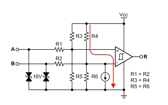
Figure 4 shows the effect of the current source connected between the B input terminal of the comparator and ground. By using the superposition principle, you can see that the current source will cause a voltage drop across R4 and R6 connected to the negative-input terminal of the comparator. This creates a fail-safe bias voltage that causes the negative terminal to have a lower voltage than the positive terminal and the output of the comparator to be in a known high state when applying a 0V differential voltage to the A and B pins.
This fail-safe biasing guarantees that the R output will be high in the presence of bus idle or bus short-circuit conditions. In the VIT numbers for the SN65HVD7x family, the positive threshold has a typical value of -70mV and the negative threshold is typically -150mV. Without fail-safe biasing, transceiver thresholds would be centered around 0V and in an indeterminate state with a 0V differential input voltage.
 Figure 4 Effect of the Offset Bias Current
In summary, understanding the basic input structures of an RS-485 receiver should help you understand important receiver electrical specifications like input-leakage current and positive and negative input thresholds. I hope you now understand the trade-offs that exist and where the numbers come from.
Stay tuned for the next RS-485 blog, which will cover the topic of unit loading. As always, feel free to post any comments or questions below.
Additional Resources
- Read other blogs in the RS-485 basics series.
- Check out the top 10 RS-485 design tips.