SSZTBT2 December 2015 ADC12J4000 , DAC38J84
** This is the ninth post in an RF-sampling blog series that appears monthly on Analog Wire. **
In my previous post, I discussed the advantages and flexibility of radio frequency (RF) sampling data converters. A high-quality clock source brings out the best performance from a data converter. This is not a new concept; while data-converter performance has always been linked with the clock source, RF sampling converters put additional strain on the clock due to high operating frequencies.
Equation Figure 1 shows the standard formula for converting clock jitter, τj, to signal-to-noise (SNR) performance:
 Figure 1 (1)
Notice that SNR is not dependent on clock frequency; it is dependent on input signal frequency. Generally, RF sampling converters work with high-frequency signals, so clock jitter plays an important role.
Total SNR performance of an analog-to-digital converter (ADC) is the combination of quantization noise, thermal noise and clock jitter, as shown in Equation Figure 1:
 Figure 2 (2)
The resolution (number of bits) of the ADC sets the quantization noise. Usually this is not the limiting factor. Thermal noise from the analog buffers and sample-and-hold circuitry set a broadband minimum threshold level. Clock-jitter contributions dominate once the input frequency increases.
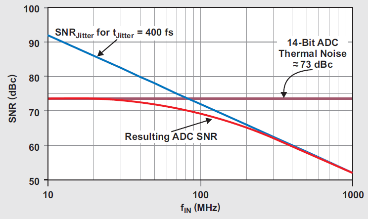
Figure 3 illustrates an SNR curve over input frequency for an ADC. The thermal noise sets the performance at low-input frequencies and jitter sets the performance at high-input frequencies.
 Figure 3 Total SNR Example from Thermal
and Jitter Contributions
Figure 3 Total SNR Example from Thermal
and Jitter ContributionsClock-jitter contributions come from aperture jitter and clock phase noise. The variation of the sampling circuitry determines the aperture jitter. The converter’s data sheet provides the aperture jitter value. For example, the aperture jitter of the ADC12J4000 ADC is 100fs. The external clock source is under your control, so providing a low-phase noise solution is critical. TI provides a simple jitter calculation worksheet that computes SNR from clock jitter and aperture jitter inputs or required clock jitter to maintain a specified SNR.
Unfortunately, low-phase-noise synthesizer sources are hard to come by. Incorporating a narrow band-pass filter centered at the clock frequency is an easy trick to improve the phase noise. The filter eliminates noise and harmonics that fall outside of the filter bandwidth. The narrower the bandwidth, the better. At lower clock frequencies, a crystal filter provides an excellent narrow filter response, usually on the order of 10kHz to 50kHz; however, crystal filters do not operate at the higher frequencies needed for RF sampling converters. For higher-frequency clocks, an LC or microstrip filter is more practical, even though they cannot achieve as narrow a bandwidth.
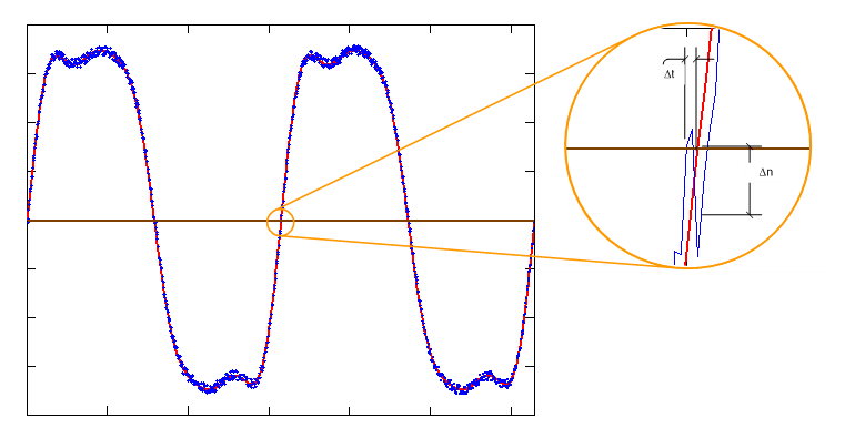
While the filter improves the phase noise, it also impacts the slew rate around the sampling points. An ideal square wave has an infinitely sharp transition. Jitter contributions in the time domain still apply, but thermal noise (which varies the amplitude) does not contribute to jitter. With a nonideal clock, the slew rate of the signal around the sampling point dictates the impact of thermal noise on the effective jitter. Figure 4 illustrates how thermal noise alters the sampling point, which translates to an error in the time domain. Incorporating a clock filter eliminates the harmonics and transforms the signal into a pure sinewave signal. The slew rate around the zero-crossing points decreases when compared to a square wave and may yield worse performance than not having the filter in place at all. Increasing the amplitude of the clock improves the slew rate around the sampling points and improves performance.
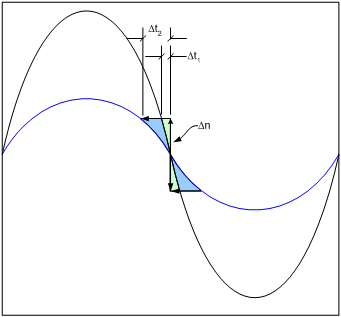
Figure 5 illustrates that a higher-amplitude sinusoid reduces the contribution of thermal noise to jitter. The clock solution commonly requires an amplitude of 10 to 15dBm to overcome filter and board losses in order to maintain a fast slew-rate signal to the converter.
 Figure 4 Thermal Noise Impact on
Clock Jitter
 Figure 5 A Higher-amplitude Signal
Generates a Higher Slew Rate
Figure 5 A Higher-amplitude Signal
Generates a Higher Slew RateSome converters include a voltage-controlled oscillator (VCO) with a phase-locked loop (PLL) to generate the clock source on-chip. You only need to provide a low-frequency reference signal, which is easy to generate and propagate across the board. For example, the DAC38J84 incorporates a VCO operating over 3.75GHz to 5.5GHz that divides down to the desired clock rate up to the converter’s maximum rate of 2.5GHz.
Generally, there will be some degradation expected with the internal PLL/VCO compared to an external source; however, you should anticipate phase-noise improvements in newer devices that rival external sources. Ultimately, the integrated PLL/VCO will be the dominant approach for providing the best performance and lowest-cost clock solution.
Check back next month, when I will introduce a new RF mixer to complement the receiver architecture.
Additional Resources
- Learn more about designing with data converters in TI’s Data Converter Learning Center.
- Read the other posts in my RF sampling blog series.
- Learn more about TI’s RF sampling ADCs.