SSZTC72 september 2015 LM25145 , LM27402 , LM27403 , LM5145 , LM5175 , LM5175-Q1
Today, in an era of intense competition, the challenge for product designers is to stay ahead of the pack and not merely walk in lockstep with it. This ups the ante for system designers to innovate with differentiated products.
One important way to innovate is with high-density designs. In the push for smaller-footprint solutions, power system designers are now focusing on the question of power density – the output power per unit of area or volume of a power converter circuit.
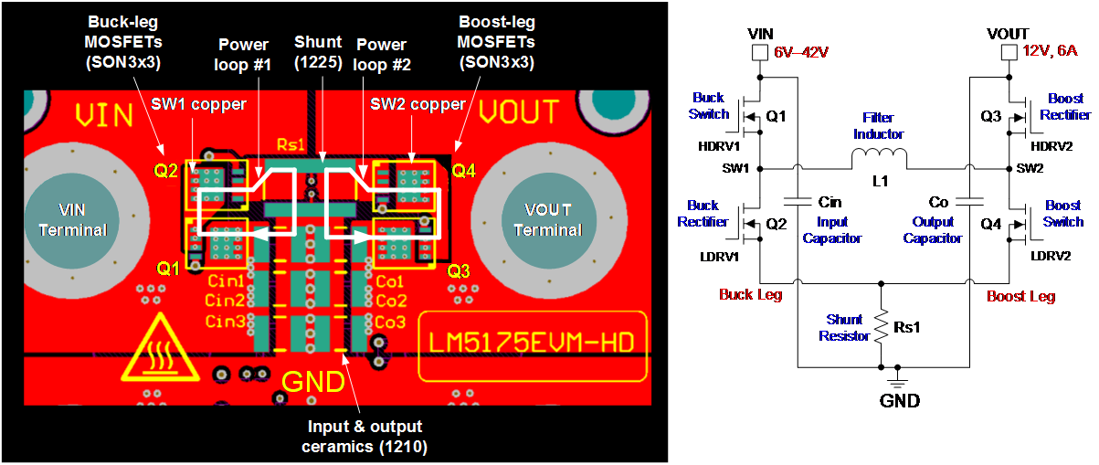
The most visible example of DC/DC converter printed circuit board (PCB) layout for high density relates to power stage component placement and routing. Careful layout can coincide with better switching performance, lower component temperatures and reduced electromagnetic interference (EMI) signatures. Consider the power stage layout and schematic in Figure 1.
 Figure 1 Four-switch Buck-boost Converter Power Stage Layout and Schematic
As I see it, these are the challenges when designing high-density DC/DC converters:
- Component technology. Advancements in component technology are key to reducing overall power dissipation, particularly at higher switching frequencies vital for filter passive component size reduction. For example, power MOSFETs have seen consistent advances in silicon and packaging, most notably with the introduction of gallium nitride (GaN) power devices with very low parasitics. Meanwhile, magnetic component performance has advanced independently, albeit at a rate arguably lagging that of power semiconductors. Prudent layout of the control IC – with integrated, adaptive gate drivers close to the MOSFETs – in many cases obviates the need for switch-node voltage slew-rate adjustment using power-dissipating snubber or gate resistor components.
- Thermal design. While a high-density layout is generally positive for conversion efficiency, it may create a thermal performance bottleneck. The same power dissipation in a smaller footprint becomes untenable. Increased component temperatures amplify concerns of higher failure rates and reliability. Lower-profile power MOSFETs placed on the top side of the PCB – not airflow-shadowed by taller components like the inductor and electrolytic capacitors – help thermal performance with convective airflow. For the converter in Figure 1, the inductor and electrolytics are purposely located on the bottom side of the multilayer PCB, because they would impede heat transfer if placed on the top.
- EMI performance. EMI regulatory compliance is a key milestone in a product’s design cycle. A high-density design typically has little space available for EMI filtering. However, tight layout improves radiated emissions as well as immunity to incoming disturbances. Two essential steps are to minimize loop areas containing high di/dt currents (see the white current paths in Figure 1) and reduce surface areas with high dv/dt voltages (see the SW1 and SW2 copper polygons in Figure 1).
- High-density PCB design flow. Clearly, it’s important for power system designers to develop and hone their PCB design skills. Even though the layout duties are often delegated to layout specialists, engineers still bear the ultimate responsibility to review the design and sign off on it.
With these challenges in mind, I recently wrote a three-part series for EDN titled “DC/DC Converter PCB Layout” that delves into PCB layout in detail. It includes a list of PCB layout guidelines structured as a checklist to aid designers during layout. The essential steps in the PCB design flow for DC/DC converters are:
- Choose the PCB structure and stack-up specification.
- Identify the high di/dt current loops and high dv/dt voltage nodes from the schematic.
- Perform power stage component layout and placement.
- Place the control IC and complete the control section layout.
- Perform critical trace routing, including MOSFET gate drive, current sense, and output-voltage feedback.
- Design the power and GND planes.
In part 2 of this blog series, I’ll unveil a high-density buck-converter layout – a 25A point-of-load design in a 20mm-by-11mm footprint.
Additional Resources:
- Read parts 1, 2 and 3 of “DC/DC Converter PCB Layout” on EDN.
- Watch a video featuring the high-density evaluation module (EVM) for the LM5175 four-switch synchronous buck-boost controller.
- Study the design equations for a buck-boost converter.
- Examine the schematic, layout and test data of these high-density buck-boost designs from the PowerLab™ reference design library:
- Start a design now with WEBENCH® Power Designer.