SSZTCB2 August 2015 LM5119
Last month, I received a customer complaint about high-frequency spikes on the output of a DC/DC converter. I first reviewed the part’s schematic locations, and all of the necessary noise filtering was in place. High-quality input bypass caps were right at the power train, the correct main waveform snubber was in place, and the output had the needed high-frequency bypass caps.
A few years ago I handled a similar complaint about another integrated DC/DC converter. I reviewed the main waveform, and it was quite clean. The input and output filtering were all in place, but large spikes appeared on the output, even when scope bandwidth was limited to 20MHz.
In both cases, looking at the layout in depth showed what was different than our evaluation modules (EVMs). In both cases, all of the layers had cutouts where the output inductor(s) were placed. This was probably done to prevent eddy current losses under the inductors. However, in both cases the breaking up of the ground plane allowed the switching pulses to reach the output. In designs with dedicated ground planes, these switching pulses are greatly attenuated at the output.
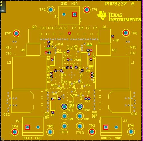
Our Power Design Services group’s practice for designs with four or more printed circuit board copper layers is to dedicate one layer (typically layer 2) to the ground plane, with no other traces allowed. We also position the feed-through holes of other potentials that could impact the ground plane to prevent or minimize cutouts. In Figure 1, which shows the PMP9227 TI Designs reference design layer 2 ground plane, the non-ground feed-throughs are spaced to ensure grounded copper between them. On boards with only two layers, the goal is to dedicate (as much as feasible) the bottom layer to the ground plane and minimize the number and length of non-ground traces on this layer.
 Figure 1 PMP9227 Layer 2 Ground Plane
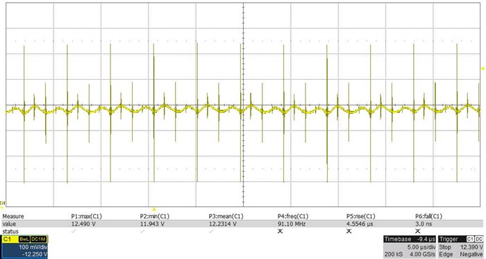
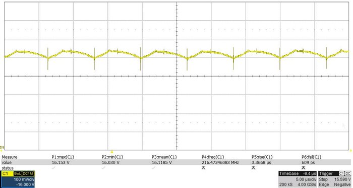
I compared two designs using the same LM5119 controller and similar speeds of main switching waveforms (~5ns rise/fall times). I tested both designs with 52VDC input and 8A loading. The PMP9227 reference design had VOUT at 16V, while the design without a ground plane had VOUT at 12V. Shown in Figure 2 & 3 are the output ripple with tip-and-barrel sensing and the scope bandwidth set to 200MHz.
Ripple out: 52VIN 12.3VOUT 8A load on PCB without ground plane: 200MHz bandwidth measurement
 Figure 2 Output Ripple/noise 200 MHz
Bandwidth in Design without Ground Plane (12V 8A off 52VIN)
Figure 2 Output Ripple/noise 200 MHz
Bandwidth in Design without Ground Plane (12V 8A off 52VIN)Ripple out: 52VIN 16VOUT 8A load on PCB with ground plane: same 200MHz measurement as in Figure 2
 Figure 3 Output Ripple/noise 200MHz
Bandwidth in the PMP9227 reference design With Ground Plane
(16V 8A off 52VIN)
Figure 3 Output Ripple/noise 200MHz
Bandwidth in the PMP9227 reference design With Ground Plane
(16V 8A off 52VIN)Figure 2 shows the output ripple in the design without the ground plane, while Figure 3 shows the output ripple for the PMP9227 reference design. Both waveforms show the same switching frequency ripple, about 30-40mV p-p. However, spikes are 530mV p-p in the first design and 120mV p-p in the PMP9227 reference design.
Taking the same measurements with 20MHz bandwidth (not shown) resulted in 140mV p-p spikes in the design without the ground plane and 10-15mV p-p spikes in the PMP9227 reference design.
With the customer who had the earlier noise issues, standard practice has become to include at least one PCB layer totally dedicated to ground. Since then with numerous designs there has not been a repeat of the noise spike issue.
Additional Resources
Read more Power Tips blogs