SSZTCC0 august 2015 SN65LBC180
Welcome back to the Get Connected blog series on Analog Wire. In my previous post, I discussed how to use low-voltage differential signal (LVDS) transceivers as a high-speed comparator in a few different applications. In this post, I’ll cover failsafe biasing of differential buses and how to implement failsafe biasing in your next design.

Bus topologies that implement more than one driver and receiver on the bus – known as multipoint – present challenges to system designers given their difference from a point-to-point bus topology. (To review bus topology architectures, see my previous blog post, “LVDS for multipoint applications.”) In multipoint applications, bus contention and idle bus conditions can cause collisions or communication glitches on the bus during normal operation. Bus contention occurs when more than one driver is active while the bus is in an indeterminate state; idle bus conditions occur when all of the drivers are in the off or Hi-Z state. The implementation of a failsafe biasing network addresses both of these situations.
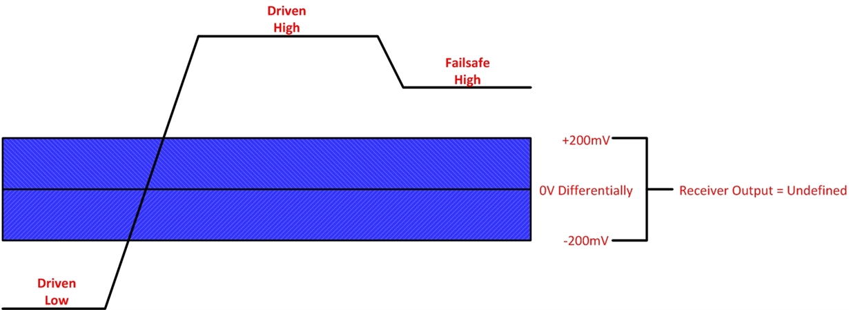
A bus that implements failsafe biasing only has two logic states in which it can exist – high and low –while a bus without failsafe biasing can exist in unknown states. An active driver will drive the bus high and low or bias it to a known state through the failsafe biasing network. Without a failsafe biasing network, the bus will reside in an unknown state in which the receiver output is invalid; noise can couple through the transceiver, causing false transitions. Figure 1 shows the possible states of a typical RS-485 bus with and without failsafe biasing.
 Figure 1 RS-485 Bus States
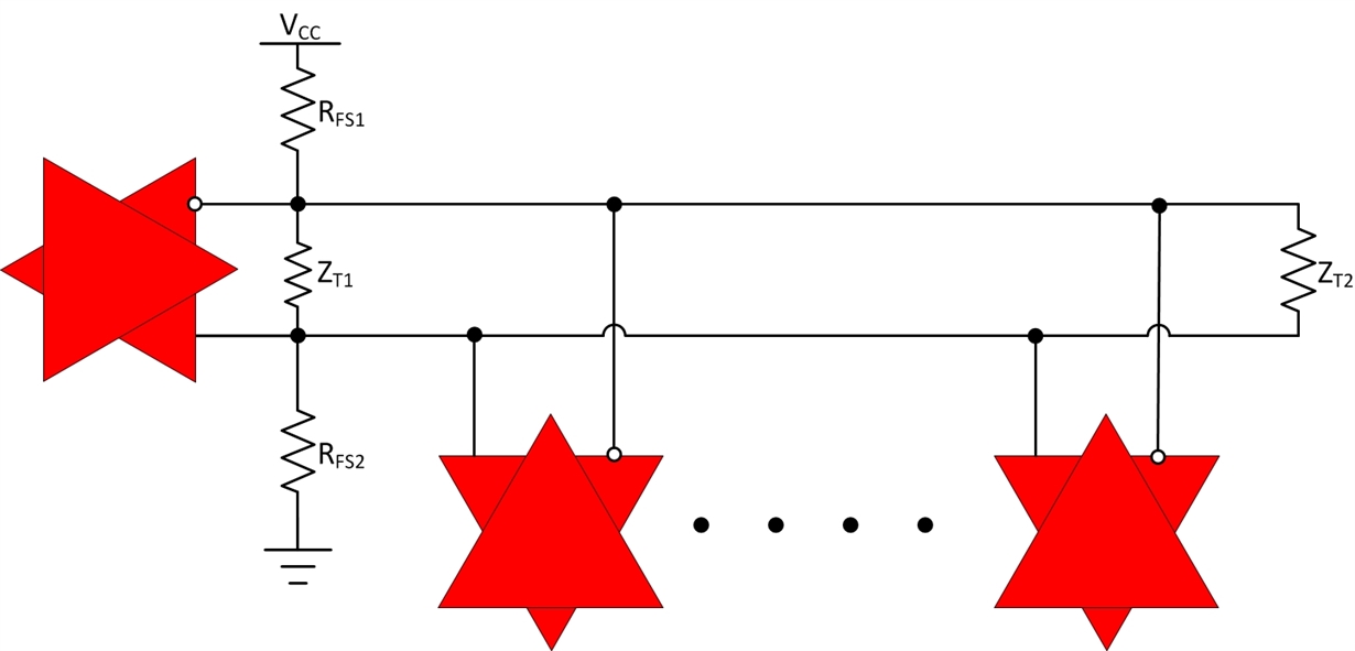
Failsafe bias resistor values are based on the maximum receiver threshold levels of the transceiver devices used in the end application, like the SN65LBC180 RS-485 transceiver. Typically for a RS-485 network the receiver input threshold level is ±200mV and for an LVDS network it is ±50mV. In addition to the receiver threshold levels, the termination resistors RFS1 and RFS2 should be equal, as that provides symmetrical loading for the drivers. The equivalent resistance of RFS1, ZT1 and RFS2 should match the characteristic impedance of the twisted-pair cable or printed circuit board (PCB) trace to maintain signal integrity (ZT1||(RFS1 + RFS2). ZT2 should also match the characteristic impedance of the network, also to maintain signal integrity, by reducing reflections on the network. Figure 2 shows a multipoint bus topology with failsafe biasing implemented.
 Figure 2 Differential Bus with Failsafe
Biasing
Figure 2 Differential Bus with Failsafe
BiasingFor more information on failsafe biasing, please see the application note, FAILSAFE Biasing of Differential Buses. Leave a comment below if you’d like to hear more about anything discussed in this post, or if there’s an interface topic you’d like to see in the future.
Additional Resources
- Read more posts in the Get Connected series.
- Check out the RS-485 full duplex evaluation module with failsafe biasing option for further bench testing.
- Find out more about TI’s RS-485 product portfolio.