SSZTCO3 may 2015 TPS54325-Q1
The duty cycle of a switching regulator is often thought of as being simply proportional to the input and output voltages. But when we look into the details of the calculations, we see that it also reflects circuit losses. Selecting components that give more losses, such as an inductor with a higher DCR, can cause the duty cycle to increase (for a buck converter), potentially resulting in additional efficiency loss from other components. When creating a power supply design with TI’s WEBENCH® Power Designer, the model calculations do not rely on basic ideal equations, but instead use detailed calculations that show you the interaction between component losses via small changes in duty cycle. To explore this, let’s look at an example of a buck converter as shown in Figure 1.
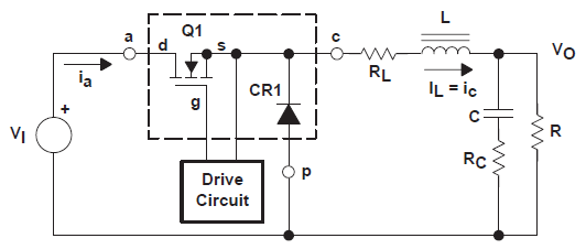 Figure 1 Asynchronous Buck
Converter.
Figure 1 Asynchronous Buck
Converter.In a buck converter duty cycle D is defined as, D = Ton/Ts
Where Ts = 1/switching frequency
Ton = switch on-time
When the high-side power switch is turned on, current drawn from the input flows through the inductor. When the high-side switch is turned off, the diode (or low-side NMOS switch in this case of a synchronous converter) is turned on and current circulates through the diode (or low-side NMOS switch) since the inductor current cannot instantaneously stop. During the steady-state operation, the on and off times of the switch are balanced to maintain the desired output voltage. Figure 2 illustrates that during on-time of the switch, inductor current and the current through the high-side MOSFET ramps up, whereas, during the off-time of the switch, the diode and inductor currents ramp down.
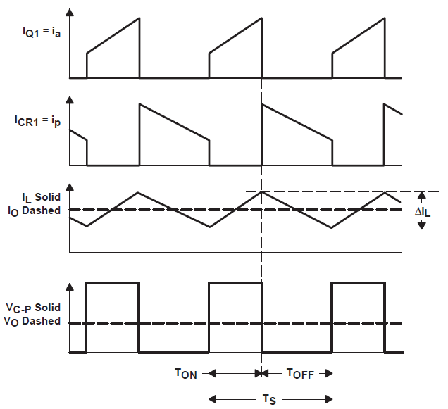 Figure 2 Buck Converter
Waveforms.
Figure 2 Buck Converter
Waveforms.Through substitution, we can get an equation for duty cycle that appears dependent on input voltage, output voltage, and the FET and diode voltage drops. If the FET and diode voltage drops are small compared to the input and output voltage, the duty cycle equation further reduces to the ratio of Vout to Vin.
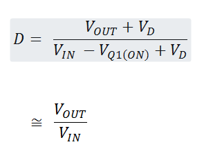
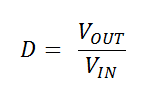

The voltage terms in the above equation are proportional to the output load current, Iout.

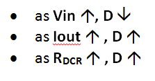
WEBENCH Power Designer calculations are based on these realistic loss terms. To study the effect of Vin, Iout and DCR on the inductor during duty cycle, a design using TI’s TPS54325-Q1 4.5V to 18V input, 3A synchronous step-down converter was created with Vin=11.5-12.5 V and Vout=3.3 V Vout @ 3A output current (see Figure 3).
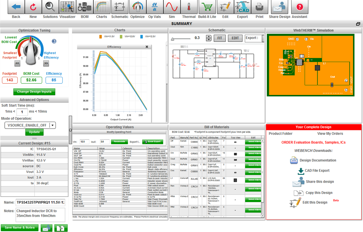 Figure 3 TPS54325-Q1 Synchronous Step-down Converter Vin=11.5-12.5V
and Vout of 3.3V @ 3A Iout Load
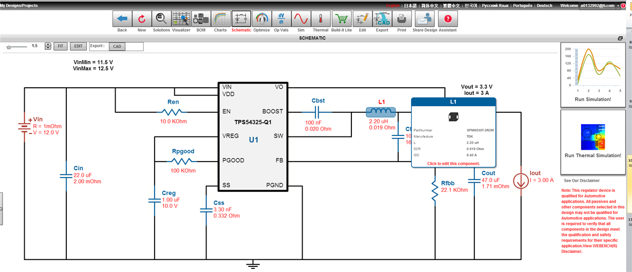 Figure 4 Notice That the Inductor
Selected Is a TDK SPM6530T-2R2M with 2.2 uH Inductance and 19 mOhm DCR
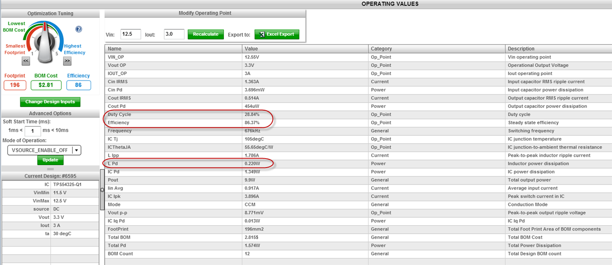 Figure 5 Calculated Operating Values of
This Design, Including Duty Cycle of 28.8%, Efficiency of 86.3% and Inductor
Power Dissipation L Pd of 0.22 W
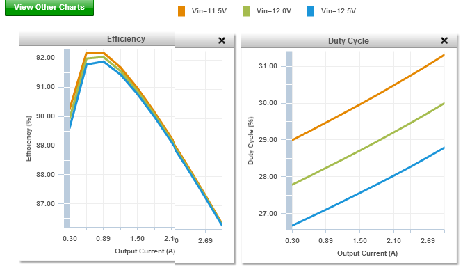 Figure 6 WEBENCH® Power Designer Charts That Confirm
That:
To study the impact of DCR on duty cycle and efficiency let’s choose a Coilcraft inductor XAL4020-222MB with the same inductance of 2.2 uH and an increased DCR of 35 mOhm(Figure 7). View the design here.
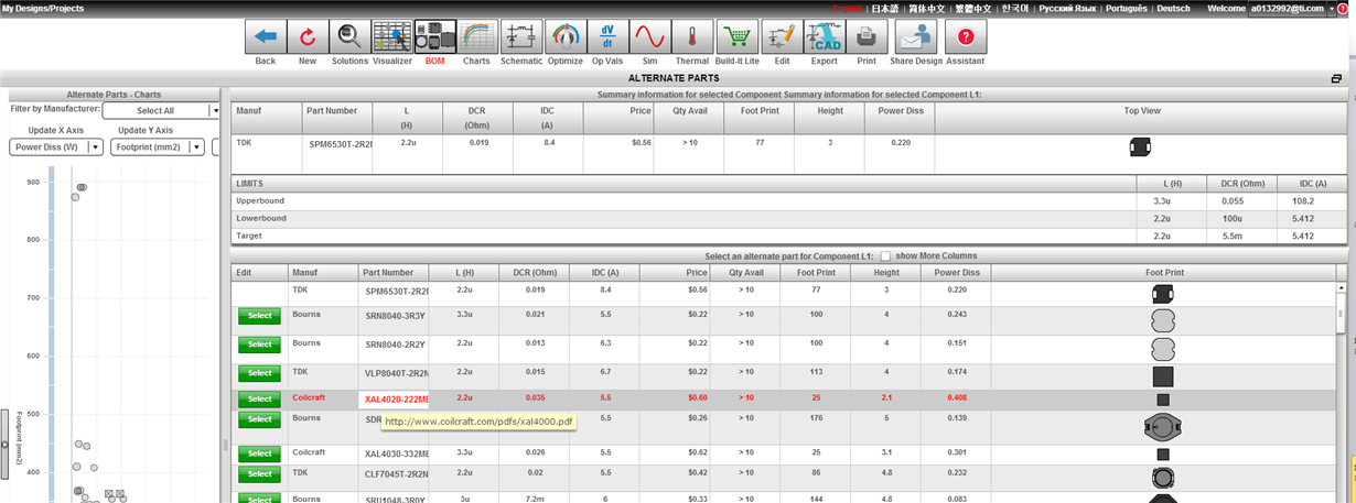 Figure 7 Selection of Coilcraft
Inductor XAL4020-222MB with the Same Inductance of 2.2 uH and an Increased DCR
of 35 mOhm
Figure 7 Selection of Coilcraft
Inductor XAL4020-222MB with the Same Inductance of 2.2 uH and an Increased DCR
of 35 mOhmWith increase in DCR the duty cycle is now 29.2% and efficiency dropped to 84.9% as seen in Figure 8.
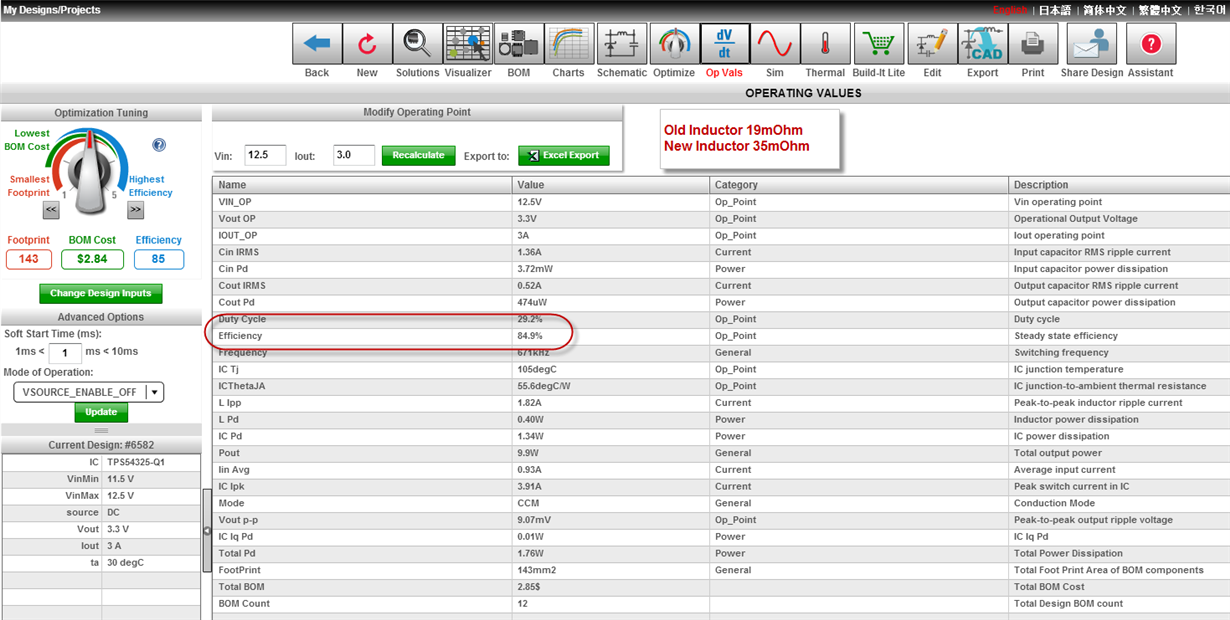 Figure 8 OpVals with Inductor with
35mOhm DCR.
Figure 8 OpVals with Inductor with
35mOhm DCR.To see a more significant change, a CUSTOM inductor with higher DCR of 0.5 W and with same inductance is selected ( Figure 9). See the design here.
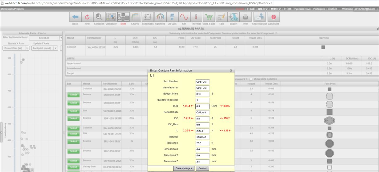 Figure 9 Setting of CUSTOM Inductor
with 0.5Ohm DCR and Same Inductance 22uH
Figure 9 Setting of CUSTOM Inductor
with 0.5Ohm DCR and Same Inductance 22uHNote that now there is a significant jump in duty cycle to 40.4% and efficiency has dropped drastically to 57%. The drop in efficiency is due to a significant rise in inductor loss to 6.08 W. Figure 10 shows the steep increase in duty cycle and sharp drop in efficiency reiterating the same.
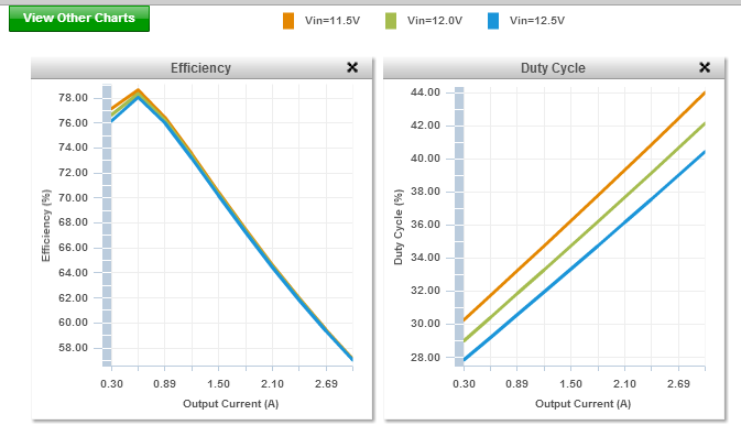 Figure 10 Efficiency and Duty Cycle
Charts Showing the Effect of CUSTOM Inductor with High DCR of 0.5Ohm
Figure 10 Efficiency and Duty Cycle
Charts Showing the Effect of CUSTOM Inductor with High DCR of 0.5OhmFigure 11 and Figure 12 summarize the three DCR cases of 19 mW, 35 mW and 0.5 W of a 2.2 uH inductor, and its impact on duty cycle, efficiency and inductor power dissipation.
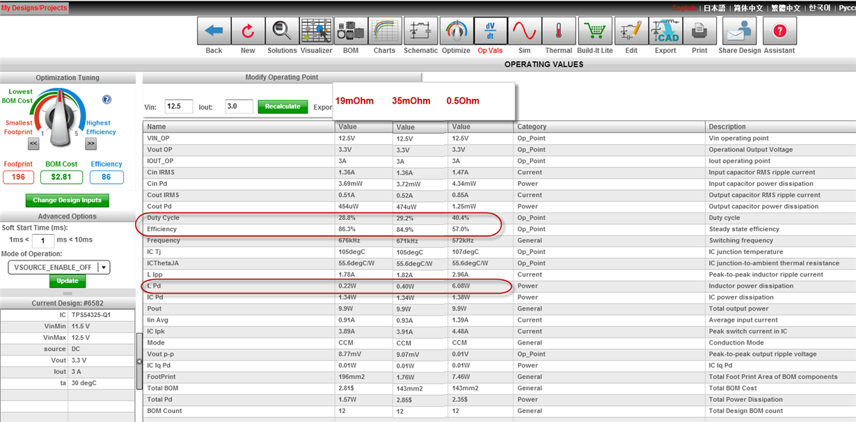 Figure 11 Comparison of OpVals for
Three Cases of DCR
 Figure 12 Summary of Charts for
Efficiency, DutyCycle and L Pd
Figure 12 Summary of Charts for
Efficiency, DutyCycle and L PdIn conclusion, the switching regulator has to work extra hard to maintain the output voltage at the desired level with increase in DCR, which results in higher power dissipation losses. It’s thus important to choose an appropriate inductor with minimal DCR to maximize the efficiency of a switching regulator with an optimal duty cycle.
Start a design in WEBENCH today or watch a video tutorial on this topic.