SSZTCZ4 September 2023 TPS61299
A device’s quiescent current, or IQ, is an important parameter for low-power, energy-efficient end equipment such as continuous blood glucose monitors (CGMs). The current drawn by the integrated circuit at light or no loads significantly influences power losses in standby mode and the total run time of the system.
The load powered by the battery is not actually always on but is a pulse-width modulation (PWM) load, meaning that the load is made up of two periods: tPWM and tStandby, shown in Figure 1. While tStandby takes up 99.9% of the total load cycle, denoted as T in Figure 1, it is still important to improve efficiency, especially light-load efficiency.
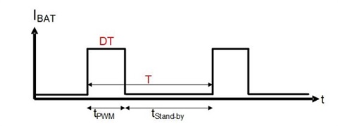 Figure 1 Load condition of a battery
system
Figure 1 Load condition of a battery
systemThe challenge is to decrease power losses in standby mode and to limit current spikes and decrease the duty cycle during the on-pulse period, thus enhancing efficiency and extending battery life. A boost converter with low IQ can help cut down the total power losses for a battery.
Choose a low-IQ boost converter to enhance overall efficiency
A CGM shows why it’s important to minimize IQ to extend battery life. Figure 2 shows a CGM power block: a sensor to read the glucose concentration, a transmitter to capture the glucose reading, and a wireless receiver for communication and display. The transmitter, consisting of a coin-cell battery, boost converter and analog front end (Figure 3) consumes the most power.
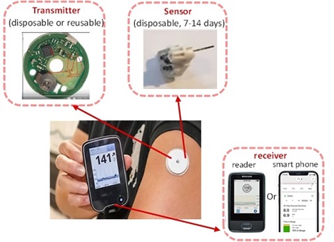 Figure 2 Power architecture of a
CGM
 Figure 3 Power architecture of a CGM
transmitter
Figure 3 Power architecture of a CGM
transmitterFigure 4 shows the load current of the analog front end. As you can see, the transmitter is in standby mode 99% of the time.
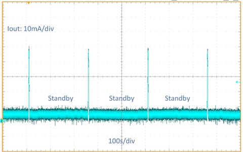 Figure 4 Current consumption vs. time
in a CGM transmitter
Figure 4 Current consumption vs. time
in a CGM transmitterEquation 1 calculates the total power supplied by the battery during one load cycle as:

Lowering the IQ could directly improve efficiency in standby mode.
TI’s TPS61299 boost converter only consumes 95 nA of IQ from VOUT, making it possible to increase efficiency 39% under the typical standby conditions of a CGM: VIN = 3.0 V, VOUT = 3.3 V and standby IOUT = 10 µA (Figure 5). An on-pulse load of 30 mA lasting 600 ms every 288-s load cycle translates to as much as 2.53 W of power saved per day. This efficiency increase in standby mode can ultimately lengthen battery life by 20%.
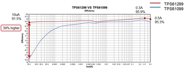 Figure 5 Efficiency curve of the
TPS61299 and a 600-nA IQ device
Figure 5 Efficiency curve of the
TPS61299 and a 600-nA IQ deviceLimit the discharge current from the battery
Although high-energy-density, low-discharge coin-cell batteries are extremely popular, their main drawback is a high equivalent series resistance (ESR) and limited current capability. For a PWM load application, the duty cycle is small, and high current pulses add to the high inrush current spikes, which are much higher than the discharge current and have detrimental effects on battery capacity and battery life – especially when using a supercapacitor. Also, as the battery ages, the ESR increases, and the power loss caused by current spikes increases accordingly.
Battery capacity is inverse with discharge current, and battery life is linear with capacity, as shown in Figure 6. Decreasing the discharge current from 500 mA to 100 mA doubles the battery life.
The TPS61299 boost converter family, available in input current limits from 5 mA to 1.5 A, accurately limits discharge current during the on-pulse period, helping prolong battery life.
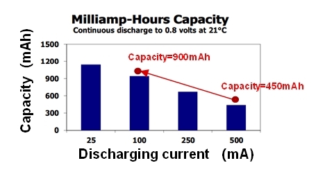 Figure 6 Battery life vs. discharge current
Select a device with fast transient response times
Decreasing the on-pulse width of the load to decrease the total power loss also extends overall battery life.
Figure 7 illustrates the load condition cycle-by-cycle of a smartwatch LED. The PWM load covers two stages: transient time (ttran) and sampling time (tsample). ttran measures how fast the boost converter regulates back to the targeted output voltage after an abrupt change in load current or supply voltage. tsample is a constant value once the photodiode settles.
Shortening ttran can largely narrow the PWM time (tPWM), widening the blanking time (tBLANK) in turn and enabling a longer low-IQ working state. Assuming that it is possible to decrease ttran from 100 µs to 10 µs, with a 10-µs tsample the cycle time is 250 µs, enabling an extension of tBLANK from 140 µs to 230 µs, as shown in Figure 8.
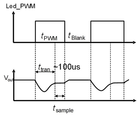 Figure 7 Traditional PWM load
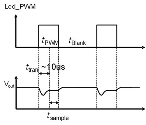 Figure 8 PWM load with fast transient
performance
Figure 8 PWM load with fast transient
performanceIt is always a struggle to maintain low IQ to achieve high efficiency during tBLANK and a shortening ttran . Low-IQ devices always suffer from longer response times because it is challenging to recharge the internal parasitic capacitors with very low IQ.
Nevertheless, the TPS61299 can achieve faster transient response times with a wider bandwidth. For example, as shown in Figure 9, the typical settling time with an output-current step up from 0 mA to 200 mA under 3.6-V input and 5-V output conditions is 8 µs.
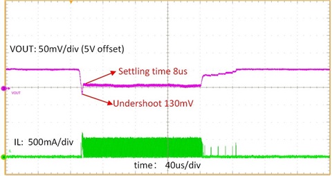 Figure 9 Transient waveform of the
TPS61299
Figure 9 Transient waveform of the
TPS61299Conclusion
The TPS61299 boost converter simultaneously integrates three of the most effective ways for designers to reduce total battery power losses:
- Choose a low-IQ boost converter to enhance overall efficiency.
- Limit the discharge current from the battery.
- Select a device with fast transient response time.
Above all, higher efficiency and lower power losses for boost converters will continue to be trends in battery applications, while lower RDS(on) and an optimized control loop may also contribute to lengthening battery life.
Additional resources
- Download the application note, “Advantages of the TPS61299 with Fast Transient Performance in Smartwatch Applications.”