SSZTD07 November 2023 AM263P4 , AM263P4-Q1

In office buildings, factory floors and automobiles, software is replacing mechanical components and fixed electric circuits. For example, replacing a mechanical lock with a smart lock gives users operational control through an app, while the manufacturer can improve or correct lock functionality through software updates. One often-forgotten challenge with this trend, however, is the increased demand placed on memory requirements.
In microcontrollers (MCUs), which typically embed flash memory, memory sizes are growing at a rapid pace. Beyond just the macro trends, there are a few specific trends in MCUs that are leading to larger flash requirements, including a higher computing bandwidth, function integration and the inclusion of additional large communication stacks. These requirements automatically double when over-the-air updates are required, as both the primary and backup image need storing.
The pressure for more memory is giving many designers “memory anxiety” – concern about running out of the memory they have on-chip. This rapid growth in memory requirements is also not sustainable both in terms of scalability and cost.
One way to address these concerns is through an external flash MCU solution.
Separating MCU and flash technologies enables the creation of a more scalable and cost-effective system. For scalability, embedded flash MCUs may require swapping to a completely different device to upgrade to more memory. For cost, as performance requirements increase and MCUs are manufactured in lower process nodes, flash simply doesn’t scale smaller like a typical digital complementary metal-oxide semiconductor (CMOS) process due to its analog components, such as the charge pump. The difficulty to scale with smaller process nodes results in paying a cost premium for embedded flash MCUs, especially for larger memory sizes (as much as $2 more for 16 MB versus external flash). However, excising flash memory from the MCU also comes with design challenges, particularly around performance, security and functional safety. To design external flash memory to obtain the cost and scalability benefits while also solving engineering challenges, TI developed OptiFlash memory technology.
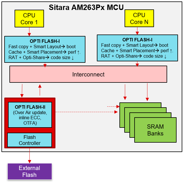
Figure 1 shows a simplified diagram of the OptiFlash technology architecture on the TI AM263P4-Q1 MCU.
 Figure 1 OptiFlash memory technology
shown on the AM263P4-Q1MCU
Figure 1 OptiFlash memory technology
shown on the AM263P4-Q1MCUWhat is OptiFlash technology?
OptiFlash technology is a combination of hardware memory controller accelerators and software tools. To address performance challenges, the AM263P4-Q1 MCU features a high-bandwidth, low-pin-count Octal Serial Peripheral Interface to the external flash integrated circuit. This interface can run at up to a 133-MHz double data rate with eight data lanes. A flash cache augmented to the external interface acts as a controller for flash instructions, placing cached instructions in on-chip RAM. Flash caching alone can improve eXecute-in-place (XIP) performance by as much as 80%, depending on the code structure.
Another common performance challenge with external flash is boot time. With a hardware boot accelerator, OptiFlash technology parallelizes portions of the boot process, resulting in initial Controller Area Network messages as fast as 56 ms or 118 ms until fully functional, depending on image size. In addition to hardware accelerators, OptiFlash technology also includes static code analysis tools such as smart placement, which profiles application code and recommends code placement in tightly coupled memory, RAM or flash, depending on execution frequency.
The inclusion of OptiFlash in devices designed to help achieve Automotive Safety Integrity Levels (ASILs) up to ASIL D and cybersecurity up to E-Safety Vehicle Intrusion Protected Applications (EVITA) Hardware Security Module (HSM) Full necessitates consideration of functional safety and security features for enabling external flash. To ensure integrity during data transfer, TI implemented inline error correcting codes into hardware in order to both detect and correct transmission errors. For security, because the flash is external, attackers could theoretically probe the data lines and read the code being executed through a man-in-the-middle attack. Encrypting the code and data on the external flash mitigates this possibility, because any data “listened” to on the line is encrypted. But because we are executing-in-place from flash, OptiFlash includes an on-the-fly authentication and encryption block to perform security functions in hardware, without any work by the user.
When combining these performance accelerators with a large on-chip RAM (3.5 MB in the AM263P4-Q1), the total performance is close to executing from on-chip RAM directly. TI benchmarking data has shown that with OptiFlash technology, the XIP performance degradation is as low as 10% more CPU cycles when compared to on-chip RAM execution.
Conclusion
As memory requirements scale higher with software-defined architectures, OptiFlash memory technology offers a paradigm shift in memory architectures to enable the scalability and cost effectiveness of external flash. This will allow for more feature-rich systems, such as the ability to get critical software updates to your vehicle through over-the-air updates or enabling a more connected system with networking that requires more space for relatively large communications stacks. By enabling more scalable and cost-effective memory storage, OptiFlash memory technology helps reduce the barriers to many emerging trends in the automotive industry.