SWCU185G January 2018 – June 2024 CC1312PSIP , CC1312R , CC1352P , CC1352R , CC2642R , CC2642R-Q1 , CC2652P , CC2652PSIP , CC2652R , CC2652RB , CC2652RSIP , CC2662R-Q1
- 1
- Read This First
-
2 Architectural Overview
- 2.1 Target Applications
- 2.2 Overview
- 2.3
Functional Overview
- 2.3.1 Arm® Cortex®-M4F
- 2.3.2 On-Chip Memory
- 2.3.3 Radio
- 2.3.4 Security Core
- 2.3.5 General-Purpose Timers
- 2.3.6 Direct Memory Access
- 2.3.7 System Control and Clock
- 2.3.8 Serial Communication Peripherals
- 2.3.9 Programmable I/Os
- 2.3.10 Sensor Controller
- 2.3.11 Random Number Generator
- 2.3.12 cJTAG and JTAG
- 2.3.13 Power Supply System
-
3 Arm® Cortex®-M4F Processor
- 3.1 Arm® Cortex®-M4F Processor Introduction
- 3.2 Block Diagram
- 3.3 Overview
- 3.4 Programming Model
- 3.5
Arm® Cortex®-M4F Core Registers
- 3.5.1 Core Register Map
- 3.5.2
Core Register Descriptions
- 3.5.2.1 Cortex®General-Purpose Register 0 (R0)
- 3.5.2.2 Cortex® General-Purpose Register 1 (R1)
- 3.5.2.3 Cortex® General-Purpose Register 2 (R2)
- 3.5.2.4 Cortex® General-Purpose Register 3 (R3)
- 3.5.2.5 Cortex® General-Purpose Register 4 (R4)
- 3.5.2.6 Cortex® General-Purpose Register 5 (R5)
- 3.5.2.7 Cortex® General-Purpose Register 6 (R6)
- 3.5.2.8 Cortex® General-Purpose Register 7 (R7)
- 3.5.2.9 Cortex® General-Purpose Register 8 (R8)
- 3.5.2.10 Cortex® General-Purpose Register 9 (R9)
- 3.5.2.11 Cortex® General-Purpose Register 10 (R10)
- 3.5.2.12 Cortex® General-Purpose Register 11 (R11)
- 3.5.2.13 Cortex® General-Purpose Register 12 (R12)
- 3.5.2.14 Stack Pointer (SP)
- 3.5.2.15 Link Register (LR)
- 3.5.2.16 Program Counter (PC)
- 3.5.2.17 Program Status Register (PSR)
- 3.5.2.18 Priority Mask Register (PRIMASK)
- 3.5.2.19 Fault Mask Register (FAULTMASK)
- 3.5.2.20 Base Priority Mask Register (BASEPRI)
- 3.5.2.21 Control Register (CONTROL)
- 3.6 Instruction Set Summary
- 3.7
Floating Point Unit (FPU)
- 3.7.1 About the FPU
- 3.7.2 FPU Functional Description
- 3.7.3 FPU Programmers Model
- 3.8 Memory Protection Unit (MPU)
- 3.9 Arm® Cortex®-M4F Processor Registers
- 4 Memory Map
- 5 Arm® Cortex®-M4F Peripherals
- 6 Interrupts and Events
-
7 JTAG Interface
- 7.1 Top-Level Debug System
- 7.2 cJTAG
- 7.3 ICEPick
- 7.4 ICEMelter
- 7.5 Serial Wire Viewer (SWV)
- 7.6 Halt In Boot (HIB)
- 7.7 Debug and Shutdown
- 7.8 Debug Features Supported Through WUC TAP
- 7.9 Profiler Register
- 7.10 Boundary Scan
- 8 Power, Reset, and Clock Management (PRCM)
- 9 Versatile Instruction Memory System (VIMS)
- 10SRAM
-
11Bootloader
- 11.1 Bootloader Functionality
- 11.2
Bootloader Interfaces
- 11.2.1 Packet Handling
- 11.2.2 Transport Layer
- 11.2.3
Serial Bus Commands
- 11.2.3.1 COMMAND_PING
- 11.2.3.2 COMMAND_DOWNLOAD
- 11.2.3.3 COMMAND_SEND_DATA
- 11.2.3.4 COMMAND_SECTOR_ERASE
- 11.2.3.5 COMMAND_GET_STATUS
- 11.2.3.6 COMMAND_RESET
- 11.2.3.7 COMMAND_GET_CHIP_ID
- 11.2.3.8 COMMAND_CRC32
- 11.2.3.9 COMMAND_BANK_ERASE
- 11.2.3.10 COMMAND_MEMORY_READ
- 11.2.3.11 COMMAND_MEMORY_WRITE
- 11.2.3.12 COMMAND_SET_CCFG
- 11.2.3.13 COMMAND_DOWNLOAD_CRC
- 12Device Configuration
-
13Cryptography
- 13.1 AES and Hash Cryptoprocessor Introduction
- 13.2 Functional Description
- 13.3 Power Management and Sleep Modes
- 13.4 Hardware Description
- 13.5 Module Description
- 13.6 AES Module Performance
- 13.7
Programming Guidelines
- 13.7.1 One-Time Initialization After a Reset
- 13.7.2 DMAC and Master Control
- 13.7.3 Hashing
- 13.7.4 Encryption and Decryption
- 13.7.5
Exceptions Handling
- 13.7.5.1 Soft Reset
- 13.7.5.2 External Port Errors
- 13.7.5.3 Key Store Errors
- 13.8 Conventions and Compliances
- 13.9 Cryptography Registers
- 14I/O Controller (IOC)
-
15Micro Direct Memory Access (µDMA)
- 15.1 μDMA Introduction
- 15.2 Block Diagram
- 15.3 Functional Description
- 15.4 Initialization and Configuration
- 15.5 µDMA Registers
- 16Timers
- 17Real-Time Clock (RTC)
- 18Watchdog Timer (WDT)
- 19True Random Number Generator (TRNG)
-
20AUX Domain Sensor Controller and Peripherals
- 20.1 Introduction
- 20.2 Power and Clock Management
- 20.3
Sensor Controller
- 20.3.1 Sensor Controller Studio
- 20.3.2 Sensor Controller Engine (SCE)
- 20.4
Digital Peripheral Modules
- 20.4.1 Overview
- 20.4.2 AIODIO
- 20.4.3 SMPH
- 20.4.4 SPIM
- 20.4.5 Time-to-Digital Converter (TDC)
- 20.4.6 Timer01
- 20.4.7
Timer2
- 20.4.7.1 Introduction
- 20.4.7.2
Functional Description
- 20.4.7.2.1 Clock Source
- 20.4.7.2.2 Clock Prescaler
- 20.4.7.2.3 Counter
- 20.4.7.2.4 Event Outputs
- 20.4.7.2.5 Channel Actions
- 20.4.7.2.6 Asynchronous Bus Bridge
- 20.5
Analog Peripheral Modules
- 20.5.1 Overview
- 20.5.2 Analog-to-Digital Converter (ADC)
- 20.5.3 COMPA
- 20.5.4 COMPB
- 20.5.5 Reference DAC
- 20.5.6 ISRC
- 20.6 Event Routing and Usage
- 20.7 Sensor Controller Alias Register Space
- 20.8
AUX Domain Sensor Controller and Peripherals Registers
- 20.8.1 ADI_4_AUX Registers
- 20.8.2 AUX_AIODIO Registers
- 20.8.3 AUX_EVCTL Registers
- 20.8.4 AUX_SMPH Registers
- 20.8.5 AUX_TDC Registers
- 20.8.6 AUX_TIMER01 Registers
- 20.8.7 AUX_TIMER2 Registers
- 20.8.8 AUX_ANAIF Registers
- 20.8.9 AUX_SYSIF Registers
- 20.8.10 AUX_SPIM Registers
- 20.8.11 AUX_MAC Registers
- 20.8.12 AUX_SCE Registers
- 21Battery Monitor and Temperature Sensor (BATMON)
-
22Universal Asynchronous Receiver/Transmitter (UART)
- 22.1 Introduction
- 22.2 Block Diagram
- 22.3 Signal Description
- 22.4 Functional Description
- 22.5 Interface to DMA
- 22.6 Initialization and Configuration
- 22.7 UART Registers
-
23Synchronous Serial Interface (SSI)
- 23.1 Introduction
- 23.2 Block Diagram
- 23.3 Signal Description
- 23.4
Functional Description
- 23.4.1 Bit Rate Generation
- 23.4.2 FIFO Operation
- 23.4.3 Interrupts
- 23.4.4
Frame Formats
- 23.4.4.1 Texas Instruments Synchronous Serial Frame Format
- 23.4.4.2 Motorola SPI Frame Format
- 23.4.4.3 Motorola SPI Frame Format With SPO = 0 and SPH = 0
- 23.4.4.4 Motorola SPI Frame Format With SPO = 0 and SPH = 1
- 23.4.4.5 Motorola SPI Frame Format With SPO = 1 and SPH = 0
- 23.4.4.6 Motorola SPI Frame Format With SPO = 1 and SPH = 1
- 23.4.4.7 MICROWIRE Frame Format
- 23.5 DMA Operation
- 23.6 Initialization and Configuration
- 23.7 SSI Registers
- 24Inter-Integrated Circuit (I2C)
-
25Inter-IC Sound (I2S)
- 25.1 Introduction
- 25.2 Block Diagram
- 25.3 Signal Description
- 25.4 Functional Description
- 25.5 Memory Interface
- 25.6 Samplestamp Generator
- 25.7 Error Detection
- 25.8 Usage
- 25.9 I2S Registers
-
26Radio
- 26.1 RF Core
- 26.2 Radio Doorbell
- 26.3
RF Core HAL
- 26.3.1 Hardware Support
- 26.3.2 Firmware Support
- 26.3.3
Command Definitions
- 26.3.3.1
Protocol-Independent Radio Operation Commands
- 26.3.3.1.1 CMD_NOP: No Operation Command
- 26.3.3.1.2 CMD_RADIO_SETUP: Set Up Radio Settings Command
- 26.3.3.1.3 CMD_FS_POWERUP: Power Up Frequency Synthesizer
- 26.3.3.1.4 CMD_FS_POWERDOWN: Power Down Frequency Synthesizer
- 26.3.3.1.5 CMD_FS: Frequency Synthesizer Controls Command
- 26.3.3.1.6 CMD_FS_OFF: Turn Off Frequency Synthesizer
- 26.3.3.1.7 CMD_RX_TEST: Receiver Test Command
- 26.3.3.1.8 CMD_TX_TEST: Transmitter Test Command
- 26.3.3.1.9 CMD_SYNC_STOP_RAT: Synchronize and Stop Radio Timer Command
- 26.3.3.1.10 CMD_SYNC_START_RAT: Synchronously Start Radio Timer Command
- 26.3.3.1.11 CMD_COUNT: Counter Command
- 26.3.3.1.12 CMD_SCH_IMM: Run Immediate Command as Radio Operation
- 26.3.3.1.13 CMD_COUNT_BRANCH: Counter Command With Branch of Command Chain
- 26.3.3.1.14 CMD_PATTERN_CHECK: Check a Value in Memory Against a Pattern
- 26.3.3.2
Protocol-Independent Direct and Immediate Commands
- 26.3.3.2.1 CMD_ABORT: ABORT Command
- 26.3.3.2.2 CMD_STOP: Stop Command
- 26.3.3.2.3 CMD_GET_RSSI: Read RSSI Command
- 26.3.3.2.4 CMD_UPDATE_RADIO_SETUP: Update Radio Settings Command
- 26.3.3.2.5 CMD_TRIGGER: Generate Command Trigger
- 26.3.3.2.6 CMD_GET_FW_INFO: Request Information on the Firmware Being Run
- 26.3.3.2.7 CMD_START_RAT: Asynchronously Start Radio Timer Command
- 26.3.3.2.8 CMD_PING: Respond With Interrupt
- 26.3.3.2.9 CMD_READ_RFREG: Read RF Core Register
- 26.3.3.2.10 CMD_SET_RAT_CMP: Set RAT Channel to Compare Mode
- 26.3.3.2.11 CMD_SET_RAT_CPT: Set RAT Channel to Capture Mode
- 26.3.3.2.12 CMD_DISABLE_RAT_CH: Disable RAT Channel
- 26.3.3.2.13 CMD_SET_RAT_OUTPUT: Set RAT Output to a Specified Mode
- 26.3.3.2.14 CMD_ARM_RAT_CH: Arm RAT Channel
- 26.3.3.2.15 CMD_DISARM_RAT_CH: Disarm RAT Channel
- 26.3.3.2.16 CMD_SET_TX_POWER: Set Transmit Power
- 26.3.3.2.17 CMD_SET_TX20_POWER: Set Transmit Power of the 20 dBm PA
- 26.3.3.2.18 CMD_UPDATE_FS: Set New Synthesizer Frequency Without Recalibration (Depricated)
- 26.3.3.2.19 CMD_MODIFY_FS: Set New Synthesizer Frequency Without Recalibration
- 26.3.3.2.20 CMD_BUS_REQUEST: Request System BUS Available for RF Core
- 26.3.3.1
Protocol-Independent Radio Operation Commands
- 26.3.4 Immediate Commands for Data Queue Manipulation
- 26.4
Data Queue Usage
- 26.4.1
Operations on Data Queues Available Only for Internal Radio CPU Operations
- 26.4.1.1 PROC_ALLOCATE_TX: Allocate TX Entry for Reading
- 26.4.1.2 PROC_FREE_DATA_ENTRY: Free Allocated Data Entry
- 26.4.1.3 PROC_FINISH_DATA_ENTRY: Finish Use of First Data Entry From Queue
- 26.4.1.4 PROC_ALLOCATE_RX: Allocate RX Buffer for Storing Data
- 26.4.1.5 PROC_FINISH_RX: Commit Received Data to RX Data Entry
- 26.4.2 Radio CPU Usage Model
- 26.4.1
Operations on Data Queues Available Only for Internal Radio CPU Operations
- 26.5
IEEE 802.15.4
- 26.5.1 IEEE 802.15.4 Commands
- 26.5.2 Interrupts
- 26.5.3 Data Handling
- 26.5.4 Radio Operation Commands
- 26.5.5 Immediate Commands
- 26.6 Bluetooth® low energy
- 26.7 Data Handling
- 26.8
Radio Operation Command Descriptions
- 26.8.1 Bluetooth® 5 Radio Setup Command
- 26.8.2 Radio Operation Commands for Bluetooth® low energy Packet Transfer
- 26.8.3 Coding Selection for Coded PHY
- 26.8.4 Parameter Override
- 26.8.5 Link Layer Connection
- 26.8.6 Slave Command
- 26.8.7 Master Command
- 26.8.8 Legacy Advertiser
- 26.8.9 Bluetooth® 5 Advertiser Commands
- 26.8.10 Scanner Commands
- 26.8.11
Initiator Command
- 26.8.11.1 Initiator Receiving Legacy Advertising Packets on Primary Channel
- 26.8.11.2 Initiator Receiving Extended Advertising Packets on Primary Channel
- 26.8.11.3 Initiator Receiving Extended Advertising Packets on Secondary Channel
- 26.8.11.4 Automatic Window Offset Insertion
- 26.8.11.5 End of Initiator Commands
- 26.8.12 Generic Receiver Command
- 26.8.13 PHY Test Transmit Command
- 26.8.14 Whitelist Processing
- 26.8.15 Backoff Procedure
- 26.8.16 AUX Pointer Processing
- 26.8.17 Dynamic Change of Device Address
- 26.9 Immediate Commands
- 26.10
Proprietary Radio
- 26.10.1 Packet Formats
- 26.10.2 Commands
- 26.10.3 Interrupts
- 26.10.4 Data Handling
- 26.10.5 Radio Operation Command Descriptions
- 26.10.6 Immediate Commands
- 26.11 Radio Registers
- 27Revision History
20.4.4.2.3 Timing Diagrams
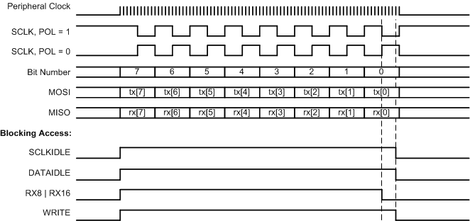
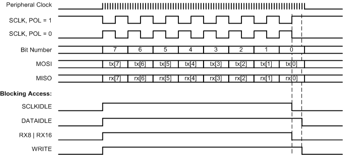
Figure 20-1 and Figure 20-14 show how the configuration of AUX_SPIM:SPIMCFG fields affect the 8-bit data transfer as well as the duration of register access blocking. For the purpose of illustration, the AUX_SPIM:SPIMCFG.DIV is set to 0x4, which gives an SCLK period that is 10 times the peripheral clock period.
In both Figure 20-13 and Figure 20-14, the peripheral clock starts to toggle and blocking begins when the user writes AUX_SPIM:TX8, which indicates the start of transmission. The value of the POL field does not impact the timing of the waveforms; it only sets the IDLE state of SCLK. The value of the PHA field determines the phase of the MOSI and MISO signals with respect to SCLK. As seen in Figure 20-13 and Figure 20-14, this also affects the blocking duration of the AUX_SPIM:SCLKIDLE register access. When PHA = 1, the access completes faster because the SCLK reaches IDLE state earlier.
Set the peripheral clock frequency with AUX_SYSIF:PEROPRATE.SPIM_OP_RATE as follows:
- When then the Sensor Controller owns the peripheral, it must be set to SCE_RATE.
- When the System CPU owns the peripheral, it must be set to BUS_RATE.
 Figure 20-13 SPI Timing Diagram: PHA = 0
 Figure 20-14 SPI Timing Diagram: PHA = 1