SWCU192 November 2021 CC1312R7 , CC1352P7 , CC2652P7 , CC2652R7
16.3.2.4 PWM Mode
The GPTM supports a simple PWM generation mode. In PWM mode, the timer is configured as a 16-bit down counter with a start value (and thus, period) defined by the GPT:TnILR and the GPT:TnPR registers. In this mode, the PWM frequency and period are synchronous events; therefore, they are ensured to be glitch-free. PWM mode is enabled with the GPT:TnMR register by setting the TnAMS bit to 0x1, setting the TnCM bit to 0x0, and setting the TnMR field to 0x2. Table 16-5 lists the values that are loaded into the timer registers when the timer is enabled.
Wait on trigger (daisy chaining) is not supported in PWM mode. The timer starts as soon as it is enabled and does not wait for a trigger from the previous timer.
| Register | Count Down Mode | Count Up Mode |
|---|---|---|
| GPT:TnR | GPT:TnILR | Not Available |
| GPT:TnV | GPT:TnILR | Not Available |
| GPT:TnPV | GPT:TnPR | Not Available |
When software writes to the GPT:CTL TnEN register bit, the counter begins counting down until it reaches the 0x0 state. Alternatively, if the GPT:TnMR TnWOT register bit is set when the TnEN bit is set, the timer waits for a trigger to begin counting. On the next counter cycle in periodic mode, the counter reloads its start value from the GPT:TnILR and the GPT:TnPR registers, and continues counting until disabled by software clearing the GPT:CTL TnEN register bit. The timer is capable of generating interrupts based on three types of events: rising edge, falling edge, or both. The event is configured by the GPT:CTL TnEVENT register field, and the interrupt is enabled by setting the GPT:TnMR TnPWMIE register bit. When the event occurs, the GPTM Raw Interrupt Status register (GPT:RIS) CnERIS bit is set, and holds the bit until it is cleared by writing the GPTM Interrupt Clear register (GPT:ICLR). If the capture mode event interrupt is enabled in the GPTM Interrupt Mask register (GPT:IMR), the GPTM also sets the GPTM Masked Interrupt Status register (GPT:MIS) CnEMIS bit.
The interrupt status bits are not updated unless the TnPWMIE bit is set.
In PWM mode, the GPT:TnR and the GPT:TnV registers always have the same value, as do the GPT:TnPS and the GPT:TnPV registers.
The output PWM signal asserts when the counter is at the value of the GPT:TnILR and the GPT:TnPR registers (its start state), and is deasserted when the counter value equals the value in the GPT:TnMATCHR and the GPT:TnPMR registers. Software can invert the output PWM signal by setting the GPT:CTL TnPWML register bit. Inverting the output PWM does not affect the edge detection interrupt. Therefore, if a positive-edge interrupt trigger has been set, the event-trigger interrupt is asserted when the PWM inversion generates a positive edge.
If TnILR is altered to a value smaller than the current counter value LD_TO_EN must be enabled to avoid transients on the PWM output. This is true even when the “Time Out UPDATE” mode is enabled.
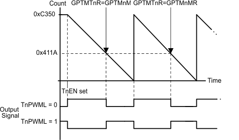
Figure 16-4 shows how to generate an output PWM with a 1-ms period and a 66% duty cycle assuming a 50 MHz input clock and TnPWML = 0 (duty cycle would be 33% for the TnPWML = 1 configuration). For this example, the start value is GPT:TnILR = 0xC350 and the match value is GPT:TnMATCHR = 0x411A.
 Figure 16-4 16-Bit PWM Mode Example
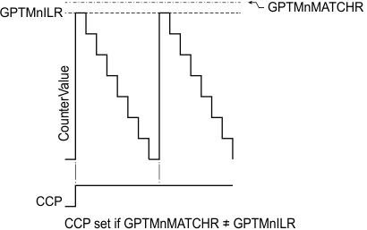
When synchronizing the timers using the GPT:SYNC register, the timer must be properly configured to avoid glitches on the CCP outputs. Both the TnPLO and the TnMRSU bits must be set in the GPT:TnMR register. Figure 16-5 shows how the CCP output operates when the TnPLO and TnMRSU bits are set and the GPT:TnMATCHR register value is greater than the GPT:TnILR register value.
 Figure 16-5 CCP Output, GPT:TnMATCHR > GPT:TnILR
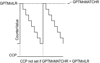
Figure 16-6 shows how the CCP output operates when the PLO and MRSU bits are set and the GPT:TnMATCHR register value is the same as the GPT:TnILR register value. In this situation, if the PLO bit is 0, the CCP signal goes high when the GPT:TnILR register value is loaded, and the match would be essentially ignored.
 Figure 16-6 CCP Output, GPT:TnMATCHR = GPT:TnILR
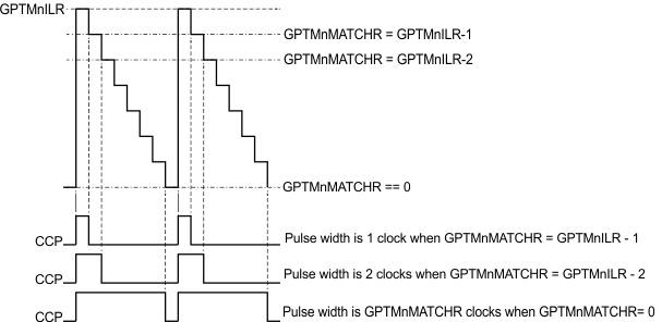
Figure 16-7 shows how the CCP output operates when the PLO and MRSU bits are set and the GPT:TnILR register value is greater than the GPT:TnMATCHR register value.
 Figure 16-7 CCP Output, GPT:TnILR > GPT:TnMATCHR