SWRS121E July 2012 – January 2016 CC2560 , CC2560B , CC2564
PRODUCTION DATA.
- 1Device Overview
- 2Revision History
- 3Device Comparison
- 4Terminal Configuration and Functions
-
5Specifications
- 5.1 Absolute Maximum Ratings
- 5.2 Recommended Operating Conditions
- 5.3 Power Consumption Summary
- 5.4 Electrical Characteristics
- 5.5
Timing and Switching Characteristics
- 5.5.1 Device Power Supply
- 5.5.2 Clock Specifications
- 5.5.3 Peripherals
- 5.5.4
RF Performance
- 5.5.4.1
Bluetooth BR/EDR RF Performance
- 5.5.4.1.1 Bluetooth Receiver—In-Band Signals
- 5.5.4.1.2 Bluetooth Receiver—General Blocking
- 5.5.4.1.3 Bluetooth Transmitter—GFSK
- 5.5.4.1.4 Bluetooth Transmitter—EDR
- 5.5.4.1.5 Bluetooth Modulation—GFSK
- 5.5.4.1.6 Bluetooth Modulation—EDR
- 5.5.4.1.7 Bluetooth Transmitter—Out-of-Band and Spurious Emissions
- 5.5.4.2 Bluetooth LE RF Performance
- 5.5.4.1
Bluetooth BR/EDR RF Performance
-
6Detailed Description
- 6.1 Overview
- 6.2 Functional Block Diagram
- 6.3 Clock Inputs
- 6.4 Functional Blocks
- 6.5 Bluetooth BR/EDR Features
- 6.6 Bluetooth LE Description
- 6.7 Bluetooth Transport Layers
- 6.8 Changes from CC2560A and CC2564 to CC2560B and CC2564B Devices
- 7Applications, Implementation, and Layout
- 8Device and Documentation Support
- 9Mechanical, Packaging, and Orderable Information
6 Detailed Description
6.1 Overview
The CC256x architecture comprises a DRP™ and a point-to-multipoint baseband core. The architecture is based on a single-processor ARM7TDMIE® core. The device includes several on-chip peripherals to enable easy communication with a host system and the Bluetooth BR/EDR/LE core.
6.2 Functional Block Diagram
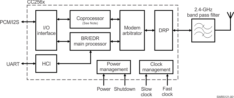
6.3 Clock Inputs
This section describes the available clock inputs. For specifications, see Section 5.5.2, Clock Specifications.
6.3.1 Slow Clock
An external source must supply the slow clock and connect to the SLOW_CLK_IN pin (for example, the host or external crystal oscillator). The source must be a digital signal in the range of 0 to 1.8 V. The accuracy of the slow clock frequency must be 32.768 kHz ±250 ppm for Bluetooth use (as specified in the Bluetooth specification). The external slow clock must be stable within 64 slow-clock cycles (2 ms) following the release of nSHUTD.
6.3.2 Fast Clock Using External Clock Source
An external clock source is fed to an internal pulse-shaping cell to provide the fast-clock signal for the device. The device incorporates an internal, automatic clock-scheme detection mechanism that automatically detects the fast-clock scheme used and configures the FREF cell accordingly. This mechanism ensures that the electrical characteristics (loading) of the fast-clock input remain static regardless of the scheme used and eliminates any power-consumption penalty-versus-scheme used.
The frequency variation of the fast-clock source must not exceed ±20 ppm (as defined by the Bluetooth specification).
The external clock can be AC- or DC-coupled, sine or square wave.
6.3.2.1 External FREF DC-Coupled
Figure 6-2 and Figure 6-3 show the clock configuration when using a square wave, DC-coupled external source for the fast clock input.
NOTE
A shunt capacitor with a range of 10 nF must be added on the oscillator output to reject high harmonics and shape the signal to be close to a sinusoidal waveform.
TI recommends using only a dedicated LDO to feed the oscillator. Do not use the same VIO for the oscillator and the CC256x device.
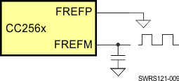 Figure 6-2 Clock Configuration (Square Wave, DC-Coupled)
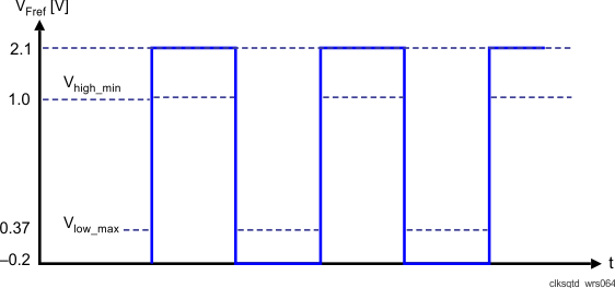 Figure 6-3 External Fast Clock (Square Wave, DC-Coupled)
Figure 6-4 and Figure 6-5 show the clock configuration when using a sine wave, DC-coupled external source for the fast clock input.
 Figure 6-4 Clock Configuration (Sine Wave, DC-Coupled)
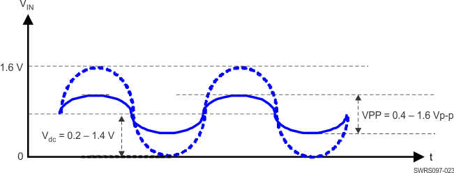 Figure 6-5 External Fast Clock (Sine Wave, DC-Coupled)
6.3.2.2 External FREF Sine Wave, AC-Coupled
Figure 6-6 and Figure 6-7 show the configuration when using a sine wave, AC-coupled external source for the fast-clock input.
 Figure 6-6 Clock Configuration (Sine Wave, AC-Coupled)
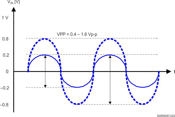 Figure 6-7 External Fast Clock (Sine Wave, AC-Coupled)
In cases where the input amplitude is greater than 1.6 Vp-p, the amplitude can be reduced to within limits. Using a small series capacitor forms a voltage divider with the internal input capacitance of approximately 2 pF to provide the required amplitude at the device input.
6.3.2.3 Fast Clock Using External Crystal
The CC256x device incorporates an internal crystal oscillator buffer to support a crystal-based fast-clock scheme. The supported crystal frequencies are 26 and 38.4 MHz.
The frequency accuracy of the fast clock source must not exceed ±20 ppm (including the accuracy of the capacitors, as specified in the Bluetooth specification).
Figure 6-8 shows the recommended fast-clock circuitry.
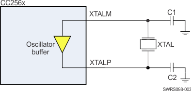 Figure 6-8 Fast-Clock Crystal Circuit
Table 6-1 lists component values for the fast-clock crystal circuit.
6.4 Functional Blocks
6.4.1 RF
The device is the third generation of TI Bluetooth single-chip devices using DRP architecture. Modifications and new features added to the DRP further improve radio performance.
Figure 6-9 shows the DRP block diagram.
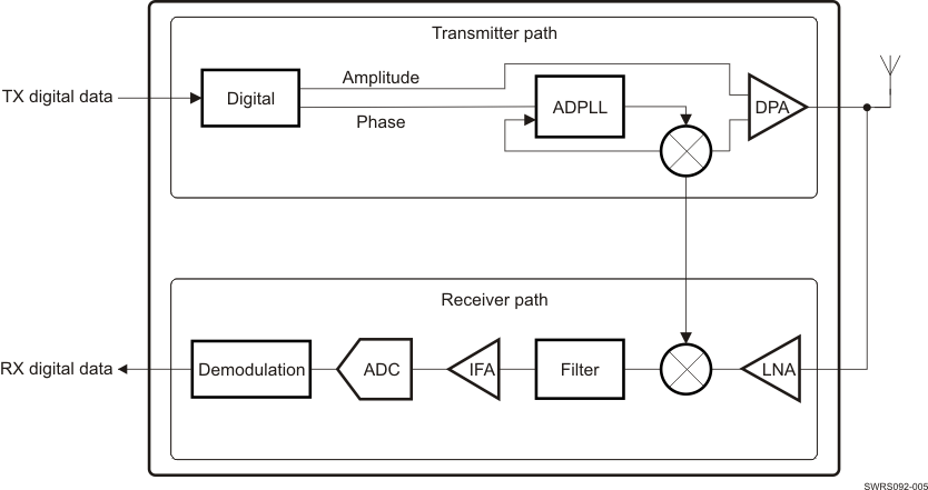 Figure 6-9 DRP Block Diagram
6.4.1.1 Receiver
The receiver uses near-zero-IF architecture to convert the RF signal to baseband data. The signal received from the external antenna is input to a single-ended low-noise amplifier (LNA) and passed to a mixer that downconverts the signal to IF, followed by a filter and amplifier. The signal is then quantized by a sigma-delta analog-to-digital converter (ADC) and further processed to reduce the interference level.
The demodulator digitally downconverts the signal to zero-IF and recovers the data stream using an adaptive-decision mechanism. The demodulator includes EDR processing with:
- State-of-the-art performance
- A maximum-likelihood sequence estimator (MLSE) to improve the performance of basic-rate GFSK sensitivity
- Adaptive equalization to enhance EDR modulation
New features include:
- LNA input range narrowed to increase blocking performance
- Active spur cancellation to increase robustness to spurs
6.4.1.2 Transmitter
The transmitter is an all-digital, sigma-delta phase-locked loop (ADPLL) based with a digitally controlled oscillator (DCO) at 2.4 GHz as the RF frequency clock. The transmitter directly modulates the digital PLL. The power amplifier is also digitally controlled. The transmitter uses the polar-modulation technique. While the phase-modulated control word is fed to the ADPLL, the amplitude-modulated controlled word is fed to the class-E amplifier to generate a Bluetooth standard-compliant RF signal.
New features include:
- Improved TX output power
- LMS algorithm to improve the differential error vector magnitude (DEVM)
6.4.2 Host Controller Interface
The CC256x device incorporates one UART module dedicated to the HCI transport layer. The HCI interface transports commands, events, and ACL between the device and the host using HCI data packets.
All members of the CC256x family supand port the H4 protocol (4-wire UART) with hardware flow control. The CC2560B and CC2564B devices also support the H5 protocol (3-wire UART) with software flow control. The CC256x device automatically detects the protocol when it receives the first command.
The maximum baud rate of the UART module is 4 Mbps; however, the default baud rate after power up is set to 115.2 kbps. The baud rate can thereafter be changed with a VS command. The device responds with a command complete event (still at 115.2 kbps), after which the baud rate change occurs.
The UART module includes the following features:
- Receiver detection of break, idle, framing, FIFO overflow, and parity error conditions
- Transmitter underflow detection
- CTS and RTS hardware flow control (H4 protocol)
- XON and XOFF software flow control (H5 protocol)
Table 6-2 lists the UART module default settings.
Table 6-2 UART Module Default Settings
| PARAMETER | VALUE |
|---|---|
| Bit rate | 115.2 kbps |
| Data length | 8 bits |
| Stop bit | 1 |
| Parity | None |
6.4.2.1 4-Wire UART Interface—H4 Protocol
The H4 UART Interface includes four signals:
- TX
- RX
- CTS
- RTS
Flow control between the host and the CC256x device is bytewise by hardware.
Figure 6-10 shows the H4 UART interface.
 Figure 6-10 H4 UART Interface
When the UART RX buffer of the device passes the flow control threshold, it sets the HCI_RTS signal high to stop transmission from the host.
When the HCI_CTS signal is set high, the device stops transmission on the interface. If HCI_CTS is set high while transmitting a byte, the device finishes transmitting the byte and stops the transmission.
The H4 protocol device includes a mechanism that handles the transition between active mode and sleep mode. The protocol occurs through the CTS and RTS UART lines and is known as the enhanced HCI low level (eHCILL) power-management protocol.
For more information on the H4 UART protocol, see Volume 4 Host Controller Interface, Part A UART Transport Layer of the Bluetooth Core Specifications (www.bluetooth.org/en-us/specification/adoptedspecifications).
6.4.2.2 3-Wire UART Interface—H5 Protocol (CC2560B and CC2564B Devices)
The H5 UART interface consists of three signals (see Figure 6-11):
- TX
- RX
- GND
 Figure 6-11 H5 UART Interface
The H5 protocol supports the following features:
- Software flow control (XON/XOFF)
- Power management using the software messages:
- WAKEUP
- WOKEN
- SLEEP
- CRC data integrity check
For more information on the H5 UART protocol, see Volume 4 Host Controller Interface, Part D Three- Wire UART Transport Layer of the Bluetooth Core Specifications (www.bluetooth.org/en-us/specification/adoptedspecifications).
6.4.3 Digital Codec Interface
The codec interface is a fully programmable port to support seamless interfacing with different PCM and I2S codec devices. The interface includes the following features:
- Two voice channels
- Master and slave modes
- All voice coding schemes defined by the Bluetooth specification: linear, A-Law, and μ-Law
- Long and short frames
- Different data sizes, order, and positions
- High flexibility to support a variety of codecs
- Bus sharing: Data_Out is in Hi-Z state when the interface is not transmitting voice data.
6.4.3.1 Hardware Interface
The interface includes four signals:
- Clock: configurable direction (input or output)
- Frame_Sync and Word_Sync: configurable direction (input or output)
- Data_In: input
- Data_Out: output or 3-state
The CC256x device can be the master of the interface when generating the Clock and Frame_Sync signals or the slave when receiving these two signals.
For slave mode, clock input frequencies of up to 15 MHz are supported. At clock rates above 12 MHz, the maximum data burst size is 32 bits.
For master mode, the device can generate any clock frequency between 64 kHz and 4.096 MHz.
6.4.3.2 I2S
When the codec interface is configured to support the I2S protocol, these settings are recommended:
- Bidirectional, full-duplex interface
- Two time slots per frame: time slot-0 for the left channel audio data; and time slot-1 for the right channel audio data
- Each time slot is configurable up to 40 serial clock cycles long, and the frame is configurable up to 80 serial clock cycles long.
6.4.3.3 Data Format
The data format is fully configurable:
- The data length can be from 8 to 320 bits in 1-bit increments when working with 2 channels, or up to 640 bits when working with 1 channel. The data length can be set independently for each channel.
- The data position within a frame is also configurable within 1 clock (bit) resolution and can be set independently (relative to the edge of the Frame_Sync signal) for each channel.
- The Data_In and Data_Out bit order can be configured independently. For example; Data_In can start with the most significant bit (MSB); Data_Out can start with the least significant bit (LSB). Each channel is separately configurable. The inverse bit order (that is, LSB first) is supported only for sample sizes up to 24 bits.
- Data_In and Data_Out are not required to be the same length.
- The Data_Out line is configured to Hi-Z output between data words. Data_Out can also be set for permanent Hi-Z, regardless of the data output. This configuration allows the device to be a bus slave in a multislave PCM environment. At power up, Data_Out is configured as Hi-Z.
6.4.3.4 Frame Idle Period
The codec interface handles frame idle periods, in which the clock pauses and becomes 0 at the end of the frame, after all data are transferred.
The device supports frame idle periods both as master and slave of the codec bus.
When the device is the master of the interface, the frame idle period is configurable. There are two configurable parameters:
- Clk_Idle_Start: indicates the number of clock cycles from the beginning of the frame to the beginning of the idle period. After Clk_Idle_Start clock cycles, the clock becomes 0.
- Clk_Idle_End: indicates the time from the beginning of the frame to the end of the idle period. The time is given in multiples of clock periods.
The delta between Clk_Idle_Start and Clk_Idle_End is the clock idle period.
For example, for clock rate = 1 MHz, frame sync period = 10 kHz, Clk_Idle_Start = 60, Clk_Idle_End = 90.
Between both Frame_Sync signals there are 70 clock cycles (instead of 100). The clock idle period starts 60 clock cycles after the beginning of the frame and lasts 90 – 60 = 30 clock cycles. Thus, the idle period ends 100 – 90 = 10 clock cycles before the end of the frame. The data transmission must end before the beginning of the idle period.
Figure 6-12 shows the frame idle timing.
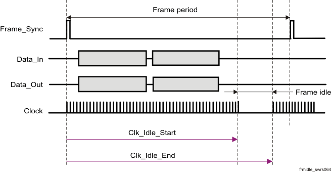 Figure 6-12 Frame Idle Period
6.4.3.5 Clock-Edge Operation
The codec interface of the device can work on the rising or the falling edge of the clock and can sample the Frame_Sync signal and the data at inversed polarity.
Figure 6-13 shows the operation of a falling-edge-clock type of codec. The codec is the master of the bus. The Frame_Sync signal is updated (by the codec) on the falling edge of the clock and is therefore sampled (by the device) on the next rising clock. The data from the codec is sampled (by the device) on the falling edge of the clock.
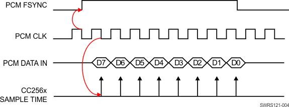 Figure 6-13 Negative Clock Edge Operation
6.4.3.6 Two-Channel Bus Example
Figure 6-14 shows a 2-channel bus in which the two channels have different word sizes and arbitrary positions in the bus frame. (FT stands for frame timer.)
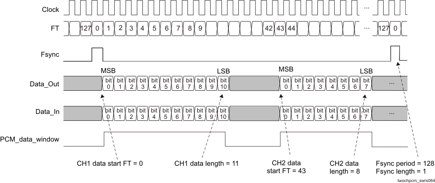 Figure 6-14 2-Channel Bus Timing
6.4.3.7 Improved Algorithm For Lost Packets
The device features an improved algorithm to improve voice quality when received voice data packets are lost. There are two options:
- Repeat the last sample: possible only for sample sizes up to 24 bits. For sample sizes larger than 24 bits, the last byte is repeated.
- Repeat a configurable sample of 8 to 24 bits (depending on the real sample size) to simulate silence (or anything else) in the bus. The configured sample is written in a specific register for each channel.
The choice between those two options is configurable separately for each channel.
6.4.3.8 Bluetooth and Codec Clock Mismatch Handling
In Bluetooth RX, the device receives RF voice packets and writes them to the codec interface. If the device receives data faster than the codec interface output allows, an overflow occurs. In this case, the Bluetooth RX has two possible modes of behavior:
- Allow overflow: if overflow is allowed, the Bluetooth RX continues receiving data and overwrites any data not yet sent to the codec.
- Do not allow overflow: if overflow is not allowed, RF voice packets received when the buffer is full are discarded.
6.4.4 Assisted Modes (CC2560B and CC2564B Devices)
The CC256x device contains an embedded coprocessor that can be used for multiple purposes (see Figure 1-1). The CC2564 and CC2564B devices use the coprocessor to perform the LE or ANT functionality. The CC256x device uses the coprocessor to execute the assisted HFP 1.6 (WBS) or assisted A2DP functions. Only one of these functions can be executed at a time because they all use the same resources (that is, the coprocessor; see Table 3-1 for the modes of operation supported by each device).
This section describes the assisted HFP 1.6 (WBS) and assisted A2DP modes of operation in the CC256x device. These modes of operation minimize host processing and power by taking advantage of the device coprocessor to perform the voice and audio SBC processing required in HFP 1.6 (WBS) and A2DP profiles. This section also compares the architecture of the assisted modes with the common implementation of the HFP 1.6 and A2DP profiles.
The assisted HFP 1.6 (WBS) and assisted A2DP modes of operation comply fully with the HFP 1.6 and A2DP Bluetooth specifications. For more information on these profiles, see the corresponding Bluetooth Profile Specification (www.bluetooth.org/en-us/specification/adopted-specifications).
6.4.4.1 Assisted HFP 1.6 (WBS)
The HFP 1.6 Profile Specification adds the requirement for WBS support. The WBS feature allows twice the voice quality versus legacy voice coding schemes at the same air bandwidth (64 kbps). This feature is achieved using a voice sampling rate of 16 kHz, a modified subband coding (mSBC) scheme, and a packet loss concealment (PLC) algorithm. The mSBC scheme is a modified version of the mandatory audio coding scheme used in the A2DP profile with the parameters listed in Table 6-3.
Table 6-3 mSBC Parameters
| PARAMETER | VALUE |
|---|---|
| Channel mode | Mono |
| Sampling rate | 16 kHz |
| Allocation method | Loudness |
| Subbands | 8 |
| Block length | 15 |
| Bitpool | 26 |
The assisted HFP 1.6 mode of operation implements this WBS feature on the embedded CC256x coprocessor. That is, the mSBC voice coding scheme and the PLC algorithm are executed in the CC256x coprocessor rather than in the host, thus minimizing host processing and power. One WBS connection at a time is supported and WBS and NBS connections cannot be used simultaneously in this mode of operation. Figure 6-15 shows the architecture comparison between the common implementation of the HFP 1.6 profile and the assisted HFP 1.6 solution.
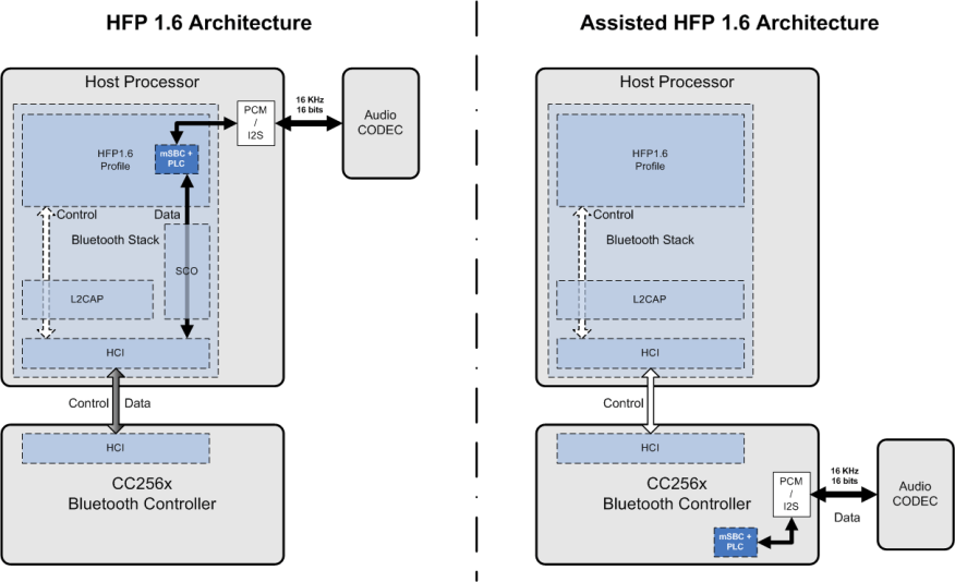 Figure 6-15 HFP 1.6 Architecture Versus Assisted HFP 1.6 Architecture
For detailed information on the HFP 1.6 profile, see the Hands-Free Profile 1.6 Specification (www.bluetooth.org/en-us/specification/adopted-specifications).
6.4.4.2 Assisted A2DP
The advanced audio distribution profile (A2DP) enables wireless transmission of high-quality mono or stereo audio between two devices. A2DP defines two roles:
- A2DP source is the transmitter of the audio stream.
- A2DP sink is the receiver of the audio stream.
A typical use case streams music from a tablet, phone, or PC (the A2DP source) to headphones or speakers (the A2DP sink). This section describes the architecture of these roles and compares them with the corresponding assisted-A2DP architecture. To use the air bandwidth efficiently, the audio data must be compressed in a proper format. The A2DP mandates support of the SBC scheme. Other audio coding algorithms can be used; however, both Bluetooth devices must support the same coding scheme. SBC is the only coding scheme spread out in all A2DP Bluetooth devices, and thus the only coding scheme supported in the assisted A2DP modes. Table 6-4 lists the recommended parameters for the SBC scheme in the assisted A2DP modes.
Table 6-4 Recommended Parameters for the SBC Scheme in Assisted A2DP Modes
| SBC ENCODER SETTINGS(1) | MID QUALITY | HIGH QUALITY | ||||||
|---|---|---|---|---|---|---|---|---|
| MONO | JOINT STEREO | MONO | JOINT STEREO | |||||
| Sampling frequency (kHz) | 44.1 | 48 | 44.1 | 48 | 44.1 | 48 | 44.1 | 48 |
| Bitpool value | 19 | 18 | 35 | 33 | 31 | 29 | 53 | 51 |
| Resulting frame length (bytes) | 46 | 44 | 83 | 79 | 70 | 66 | 119 | 115 |
| Resulting bit rate (Kbps) | 127 | 132 | 229 | 237 | 193 | 198 | 328 | 345 |
The SBC scheme supports a wide variety of configurations to adjust the audio quality. Table 6-5 through Table 6-12 list the supported SBC capabilities in the assisted A2DP modes.
Table 6-5 Channel Modes
| CHANNEL MODE | STATUS |
|---|---|
| Mono | Supported |
| Dual channel | Supported |
| Stereo | Supported |
| Joint stereo | Supported |
Table 6-6 Sampling Frequency
| SAMPLING FREQUENCY (kHz) | STATUS |
|---|---|
| 16 | Supported |
| 44.1 | Supported |
| 48 | Supported |
Table 6-10 Bitpool Values
| BITPOOL RANGE | STATUS |
|---|---|
| Assisted A2DP sink: 2–54 | Supported |
| Assisted A2DP source: 2–57 | Supported |
Table 6-11 L2CAP MTU Size
| L2CAP MTU SIZE (BYTES) | STATUS |
|---|---|
| Assisted A2DP sink: 260–800 | Supported |
| Assisted A2DP source: 260–1021 | Supported |
Table 6-12 Miscellaneous Parameters
| ITEM | VALUE | STATUS |
|---|---|---|
| A2DP content protection | Protected | Not supported |
| AVDTP service | Basic type | Supported |
| L2CAP mode | Basic mode | Supported |
| L2CAP flush | Nonflushable | Supported |
For detailed information on the A2DP profile, see the A2DP Profile Specification at Adopted Bluetooth Core Specifications.
6.4.4.2.1 Assisted A2DP Sink
The A2DP sink role is the receiver of the audio stream in an A2DP Bluetooth connection. In this role, the A2DP layer and its underlying layers are responsible for link management and data decoding. To handle these tasks, two logic transports are defined:
- Control and signaling logic transport
- Data packet logic transport
The assisted A2DP takes advantage of this modularity to handle the data packet logic transport in the CC256x device by implementing a light L2CAP layer (L-L2CAP) and light AVDTP layer (L-AVDTP) to defragment the packets. Then the assisted A2DP performs the SBC decoding on-chip to deliver raw audio data through the CC256x PCM–I2S interface. Figure 6-16 shows the comparison between a common A2DP sink architecture and the assisted A2DP sink architecture.
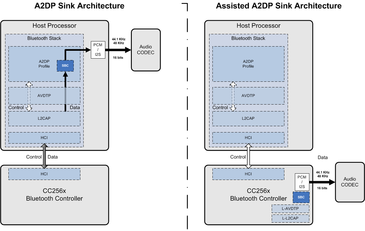 Figure 6-16 A2DP Sink Architecture Versus Assisted A2DP Sink Architecture
For more information on the A2DP sink role, see the A2DP Profile Specification at Adopted Bluetooth Core Specifications.
6.4.4.2.2 Assisted A2DP Source
The role of the A2DP source is to transmit the audio stream in an A2DP Bluetooth connection. In this role, the A2DP layer and its underlying layers are responsible for link management and data encoding. To handle these tasks, two logic transports are defined:
- Control and signaling logic transport
- Data packet logic transport
The assisted A2DP takes advantage of this modularity to handle the data packet logic transport in the CC256x device. First, the assisted A2DP encodes the raw data from the CC256x PCM–I2S interface using an on-chip SBC encoder. The assisted A2DP then implements an L-L2CAP layer and an L-AVDTP layer to fragment and packetize the encoded audio data. Figure 6-17 shows the comparison between a common A2DP source architecture and the assisted A2DP source architecture.
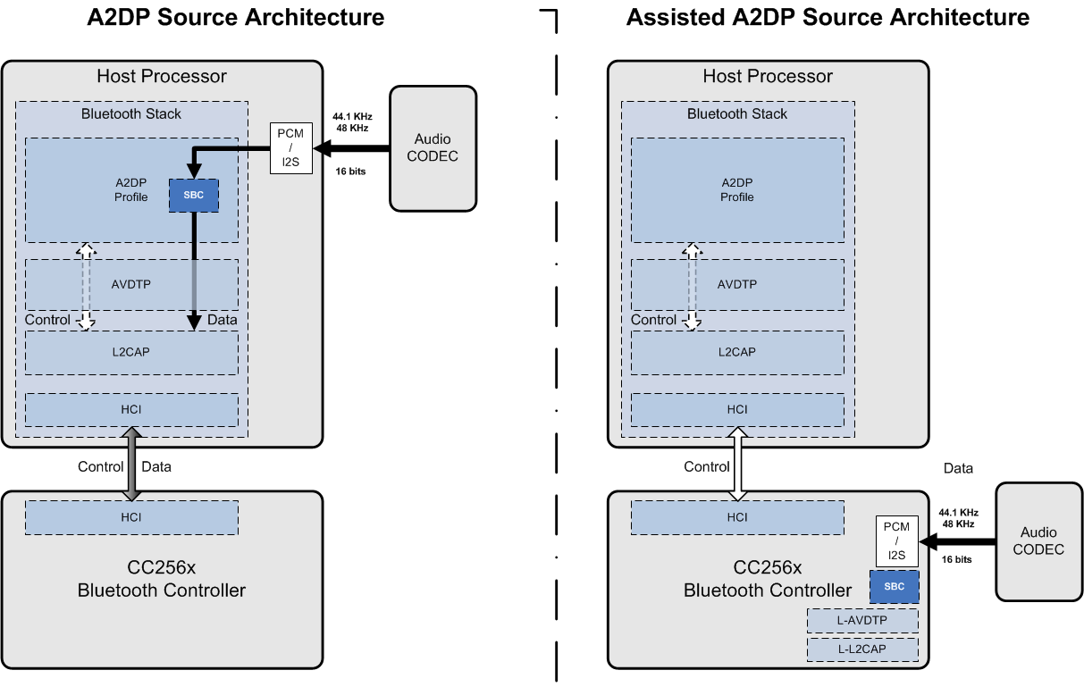 Figure 6-17 A2DP Source Architecture Versus Assisted A2DP Source Architecture
For more information on the A2DP source role, see the A2DP Profile Specification at Adopted Bluetooth Core Specifications.
6.5 Bluetooth BR/EDR Features
The CC2564B/CC2560B devices fully comply with the Bluetooth 4.0 specification up to the HCI level. The CC2560B/CC2564B devices are compliant with the Bluetooth 4.1 specification up to the HCI layer (for family members and technology supported, see Table 3-1):
- Up to seven active devices
- Scatternet: Up to 3 piconets simultaneously, 1 as master and 2 as slaves
- Up to two synchronous connection oriented (SCO) links on the same piconet
- Very fast AFH algorithm for asynchronous connection-oriented link (ACL) and extended SCO (eSCO) link
- Supports typical 12-dBm TX power without an external power amplifier (PA), thus improving Bluetooth link robustness
- Digital radio processor (DRP™) single-ended 50-Ω I/O for easy RF interfacing
- Internal temperature detection and compensation to ensure minimal variation in RF performance over temperature
- Includes a 128-bit hardware encryption accelerator as defined by the Bluetooth specifications
- Flexible pulse-code modulation (PCM) and inter-IC sound (I2S) digital codec interface:
- Full flexibility of data format (linear, A-Law, μ-Law)
- Data width
- Data order
- Sampling
- Slot positioning
- Master and slave modes
- High clock rates up to 15 MHz for slave mode (or 4.096 MHz for master mode)
- Support for all voice air-coding
- CVSD
- A-Law
- μ-Law
- Transparent (uncoded)
- The CC2560B and CC2564B devices provide an assisted mode for the HFP 1.6 (wide-band speech [WBS]) profile or A2DP profile to reduce host processing and power.
6.6 Bluetooth LE Description
The CC2564B device fully complies with the Bluetooth 4.0 specification up to the HCI level. The CC2564B device is Bluetooth 4.1 specification compliant up to the HCI layer (for the family members and technology supported, see Table 3-1):
- Solution optimized for proximity and sports use cases
- Supports up to 10 (CC2564B) simultaneous connections
- Multiple sniff instances that are tightly coupled to achieve minimum power consumption
- Independent buffering for LE, allowing large numbers of multiple connections without affecting BR/EDR performance
- Built-in coexistence and prioritization handling
NOTE
ANT and the assisted modes (HFP 1.6 and A2DP) are not available when BLE is enabled.
6.7 Bluetooth Transport Layers
Figure 6-18 shows the Bluetooth transport layers.
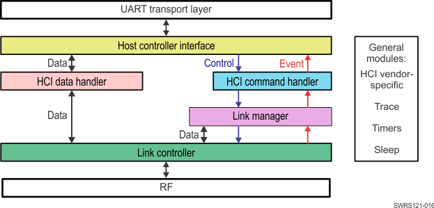 Figure 6-18 Bluetooth Transport Layers
6.8 Changes from CC2560A and CC2564 to CC2560B and CC2564B Devices
The CC2560B and CC2564B devices include the following changes from the CC2560A and CC2564 devices:
- From a hardware perspective, both devices are pin compatible. From a software perspective, each device requires a different service pack. When operating with the two devices using the supported Bluetooth stack, the devices are integrated seamlessly and use remains identical for each device.
- Assisted mode for the HFP 1.6 (WBS) profile or the A2DP profile to enable more advanced features without using host processing or power
- Support for the H5 protocol in the UART transport layer using 2-wire UART
- Enable 10 Bluetooth LE connections