SWRS121E July 2012 – January 2016 CC2560 , CC2560B , CC2564
PRODUCTION DATA.
- 1Device Overview
- 2Revision History
- 3Device Comparison
- 4Terminal Configuration and Functions
-
5Specifications
- 5.1 Absolute Maximum Ratings
- 5.2 Recommended Operating Conditions
- 5.3 Power Consumption Summary
- 5.4 Electrical Characteristics
- 5.5
Timing and Switching Characteristics
- 5.5.1 Device Power Supply
- 5.5.2 Clock Specifications
- 5.5.3 Peripherals
- 5.5.4
RF Performance
- 5.5.4.1
Bluetooth BR/EDR RF Performance
- 5.5.4.1.1 Bluetooth Receiver—In-Band Signals
- 5.5.4.1.2 Bluetooth Receiver—General Blocking
- 5.5.4.1.3 Bluetooth Transmitter—GFSK
- 5.5.4.1.4 Bluetooth Transmitter—EDR
- 5.5.4.1.5 Bluetooth Modulation—GFSK
- 5.5.4.1.6 Bluetooth Modulation—EDR
- 5.5.4.1.7 Bluetooth Transmitter—Out-of-Band and Spurious Emissions
- 5.5.4.2 Bluetooth LE RF Performance
- 5.5.4.1
Bluetooth BR/EDR RF Performance
-
6Detailed Description
- 6.1 Overview
- 6.2 Functional Block Diagram
- 6.3 Clock Inputs
- 6.4 Functional Blocks
- 6.5 Bluetooth BR/EDR Features
- 6.6 Bluetooth LE Description
- 6.7 Bluetooth Transport Layers
- 6.8 Changes from CC2560A and CC2564 to CC2560B and CC2564B Devices
- 7Applications, Implementation, and Layout
- 8Device and Documentation Support
- 9Mechanical, Packaging, and Orderable Information
9 Mechanical, Packaging, and Orderable Information
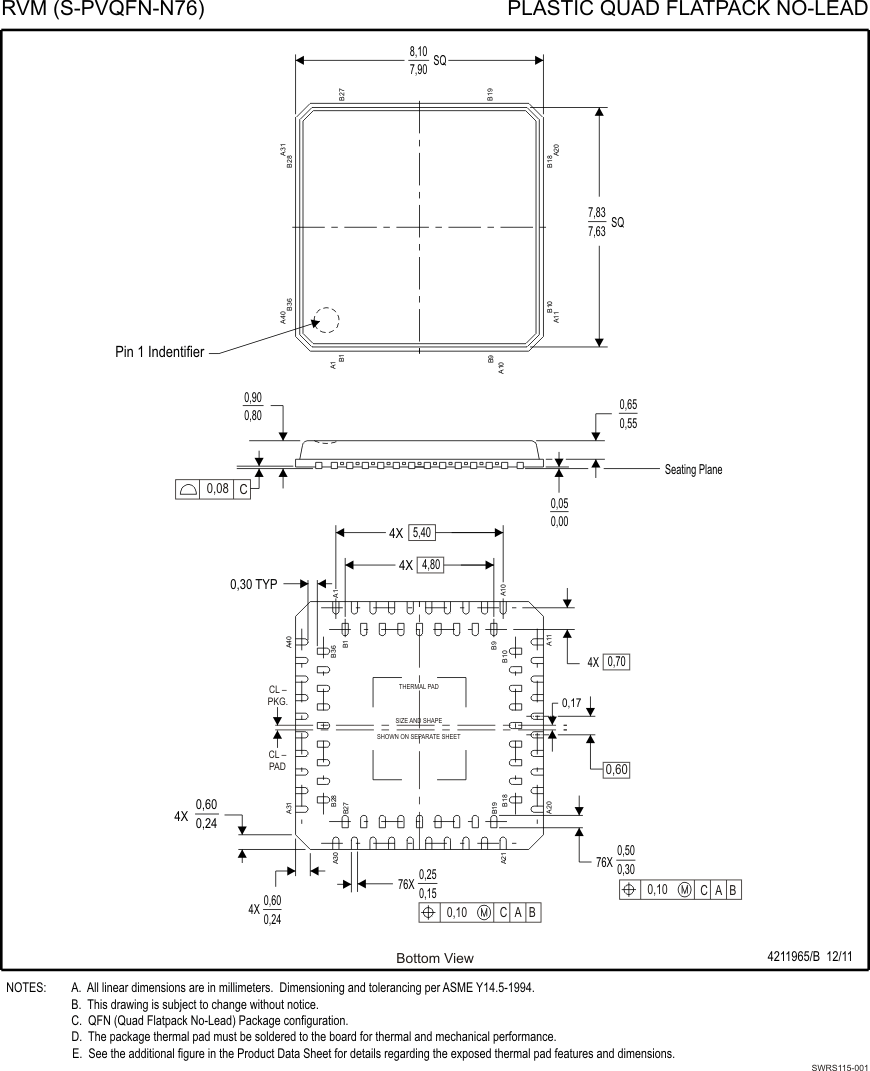
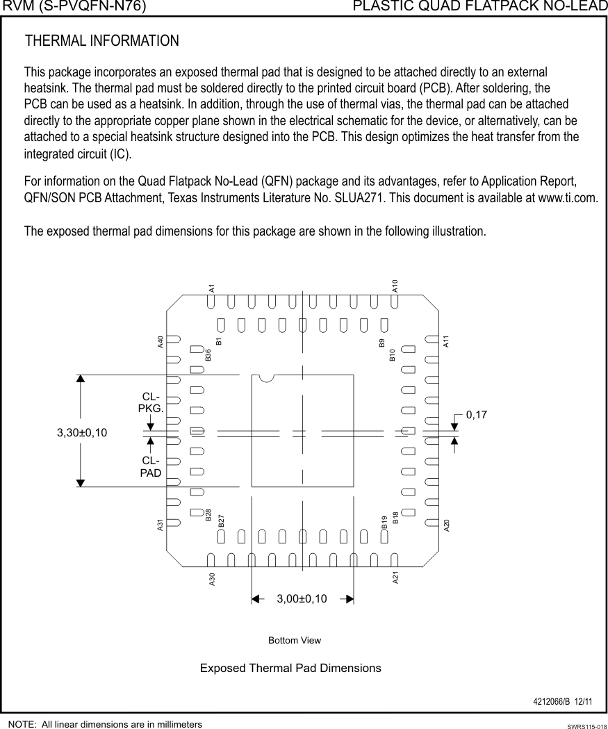
The following pages include mechanical packaging and orderable information. This information is the most current data available for the designated devices. This data is subject to change without notice and revision of this document. For browser-based versions of this data sheet, refer to the left-hand navigation.
9.1 mrQFN Mechanical Data
9.2 Packaging and Ordering
9.2.1 Package and Ordering Information
The mrQFN packaging is 76 pins and a 0.6-mm pitch.
For detailed information, see Section 9.1, mrQFN Mechanical Data.
Table 9-1 lists the package and order information for the device family members.
Table 9-1 Package and Order Information
| DEVICE | PACKAGE SUFFIX | PIECES/REEL |
|---|---|---|
| CC2560ARVMT (NRND)(1) | RVM | 250 |
| CC2560ARVMR (NRND)(1) | RVM | 2500 |
| CC2564RVMT (NRND)(1) | RVM | 250 |
| CC2564RVMR (NRND)(1) | RVM | 2500 |
| CC2560BRVMT | RVM | 250 |
| CC2560BRVMR | RVM | 2500 |
| CC2564BRVMT | RVM | 250 |
| CC2564BRVMR | RVM | 2500 |
Figure 9-1 shows the markings for the CC256x family.
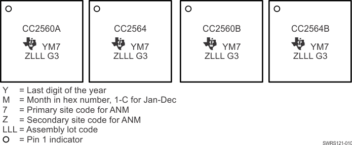 Figure 9-1 Chip Markings
9.2.2 Empty Tape Portion
Figure 9-2 shows the empty portion of the carrier tape.
 Figure 9-2 Carrier Tape and Pockets
9.2.3 Device Quantity and Direction
When pulling out the tape, the A1 corner is on the left side (see Figure 9-3).
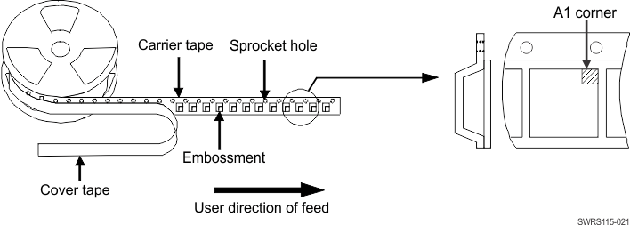 Figure 9-3 Direction of Device
9.2.4 Insertion of Device
Figure 9-4 shows the insertion of the device.
 Figure 9-4 Insertion of Device
9.2.5 Tape Specification
The dimensions of the tape are:
- Tape width: 16 mm
- Cover tape: The cover tape does not cover the index hole and does not shift to outside from the carrier tape.
- Tape structure: The carrier tape is made of plastic. The device is put in the embossed area of the carrier tape and covered by the cover tape, which is made of plastic.
- ESD countermeasure: The plastic material used in the carrier tape and the cover tape is static dissipative.
9.2.6 Reel Specification
Figure 9-5 shows the reel specifications:
- 330-mm reel, 16-mm width tape
- Reel material: Polystyrene (static dissipative/antistatic)
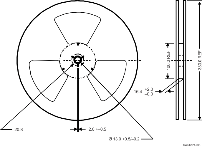 Figure 9-5 Reel Dimensions (mm)
9.2.7 Packing Method
The end of the leader tape is secured by drafting tape. The reel is packed in a moisture barrier bag fastened by heat-sealing (see Figure 9-6).
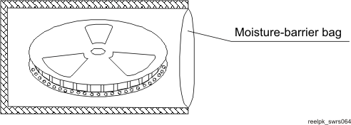 Figure 9-6 Reel Packing Method
CAUTION
This integrated circuit can be damaged by ESD. Texas Instruments recommends that all integrated circuits be handled with appropriate precautions. Failure to observe proper handling and installation procedures can cause damage. ESD damage can range from subtle performance degradation to complete device failure. Precision integrated circuits may be more susceptible to damage because very small parametric changes could cause devices not to meet their published specifications.
9.2.8 Packing Specification
9.2.8.1 Reel Box
Each moisture-barrier bag is packed into a reel box, as shown in Figure 9-7.
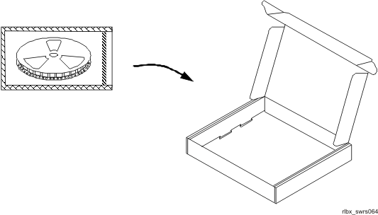 Figure 9-7 Reel Box (Carton)
9.2.8.2 Reel Box Material
The reel box is made from corrugated fiberboard.
9.2.8.3 Shipping Box
If the shipping box has excess space, filler (such as cushion) is added.
Figure 9-8 shows a typical shipping box.
NOTE
The size of the shipping box may vary depending on the number of reel boxes packed.
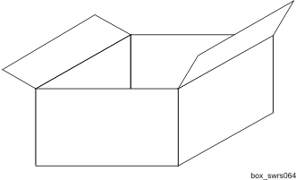 Figure 9-8 Shipping Box (Carton)
9.2.8.4 Shipping Box Material
The shipping box is made from corrugated fiberboard.