SWRU359F September 2015 – December 2021 WL1801MOD , WL1805MOD , WL1831MOD , WL1835MOD
7.1 Board Layout
Figure 7-1 shows the WL1835MODCOM8B 4-layer board. Table 7-1, Figure 7-2, Figure 7-3, Figure 7-4, Figure 7-5, and Figure 7-6 show instances of good layout practices.
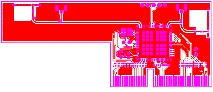 Figure 7-1 Layer
1
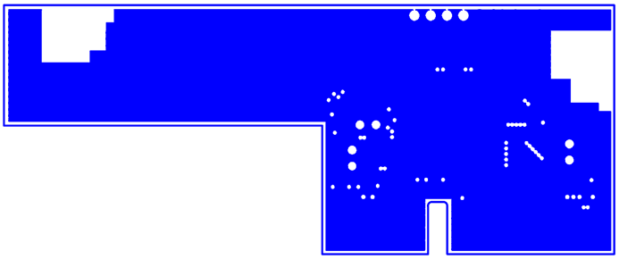 Figure 7-2 Layer
2
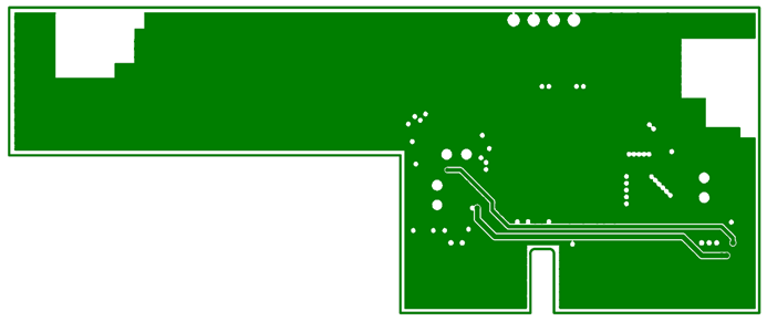 Figure 7-3 Layer
3
 Figure 7-4 Layer
4
Figure 7-4 Layer
4| Reference | Guideline Description |
|---|---|
| 1 | The proximity of ground vias must be close to the pad. |
| 2 | Signal traces must not be run underneath the module on the layer where the module is mounted. |
| 3 | Have a complete ground pour in layer 2 for thermal dissipation. |
| 4 | Have a solid ground plane and ground vias under the module for stable system and thermal dissipation. |
| 5 | Increase the ground pour in the first layer and have all of the traces from the first layer on the inner layers, if possible. |
| 6 | Signal traces can be run on a third layer under the solid ground layer, which is below the module mounting layer. |
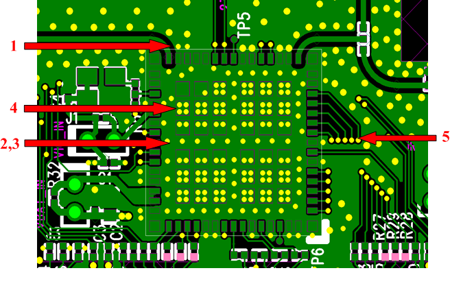 Figure 7-5 Module
Layout Guidelines (Top Layer)
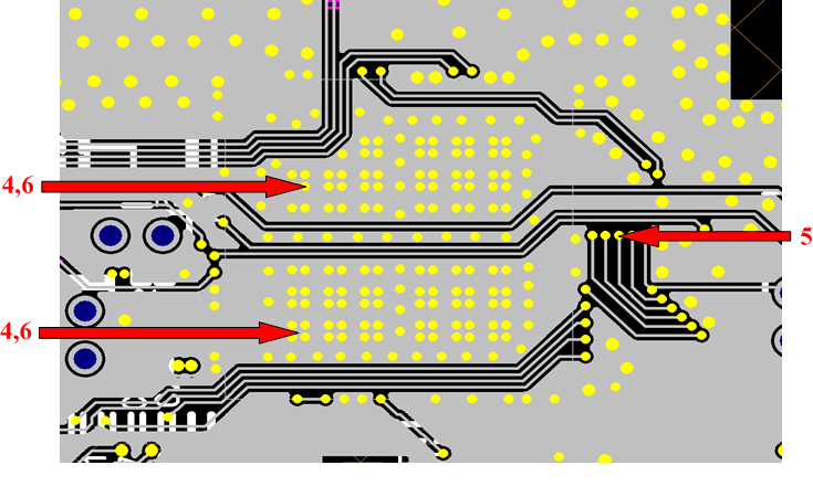 Figure 7-6 Module
Layout Guidelines (Bottom Layer)
Figure 7-6 Module
Layout Guidelines (Bottom Layer)Figure 7-7 shows the trace design for the PCB. A 50-Ω impedance match on the trace to the antenna should be used. Also, 50-Ω traces are recommended for the PCB layout.
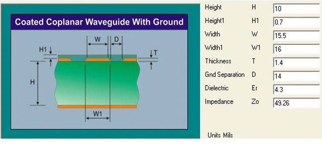 Figure 7-7 Trace
Design for the PCB Layout
Figure 7-7 Trace
Design for the PCB LayoutFigure 7-8 shows layer 1 with the trace to the antenna over ground layer 2.
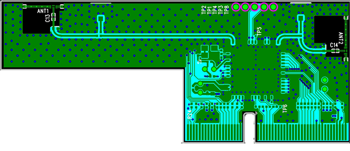 Figure 7-8 Layer 1
Combined With Layer 2
Figure 7-8 Layer 1
Combined With Layer 2Table 7-2, Figure 7-9, and Figure 7-10 describe instances of good layout practices for the antenna and RF trace routing.
| Reference | Guideline Description |
|---|---|
| 1 | The RF trace antenna feed must be as short as possible beyond the ground reference. At this point, the trace starts to radiate. |
| 2 | The RF trace bends must be gradual with an approximate maximum bend of 45 degrees with trace mitered. RF traces must not have sharp corners. |
| 3 | RF traces must have via stitching on the ground plane beside the RF trace on both sides |
| 4 | RF traces must have constant impedance (microstrip transmission line). |
| 5 | For best results, the RF trace ground layer must be the ground layer immediately below the RF trace. The ground layer must be solid. |
| 6 | There must be no traces or ground under the antenna section. |
| 7 | RF traces must be as short as possible. The antenna, RF traces, and modules must be on the edge of the PCB product. The proximity of the antenna to the enclosure and the enclosure material must also be considered. |
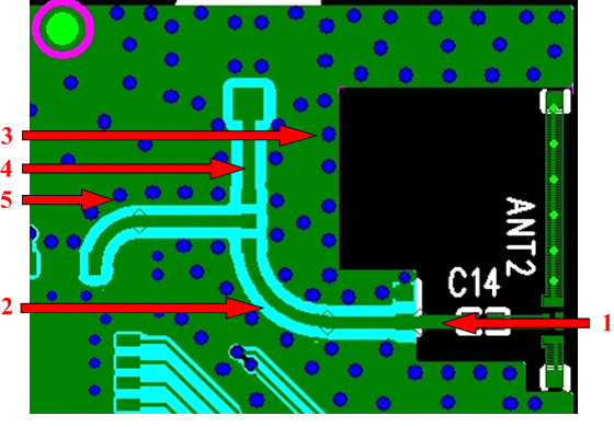 Figure 7-9 Top Layer
– Antenna and RF Trace Routing Layout Guidelines
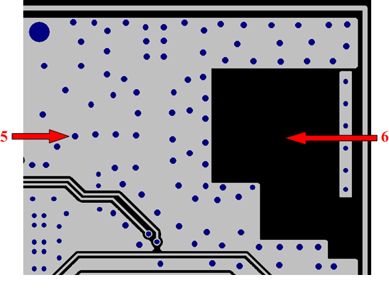 Figure 7-10 Bottom
Layer – Antenna and RF Trace Routing Layout Guidelines
Figure 7-10 Bottom
Layer – Antenna and RF Trace Routing Layout GuidelinesFigure 7-11 describes the MIMO antenna spacing. The distance of ANT1 and ANT2 must be greater than half of wavelength (62.5 mm at 2.4 GHz).
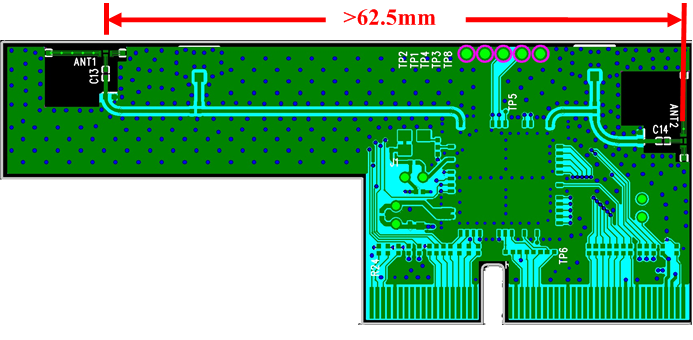 Figure 7-11 MIMO
Antenna Spacing
Figure 7-11 MIMO
Antenna SpacingThe supply routing guidelines are as follows:
- For power supply routing, the power trace for VBAT must be at least 40-mil wide.
- The 1.8-V trace must be at least 18-mil wide.
- Make VBAT traces as wide as possible to ensure reduced inductance and trace resistance.
- If possible, shield VBAT traces with ground above, below, and beside the traces.
The digital-signal routing guidelines are as follows:
- Route SDIO signal traces (CLK, CMD, D0, D1, D2, and D3) in parallel to each other and as short as possible (less than 12 cm). In addition, each trace must be the same length. Ensure enough space between traces (greater than 1.5 times the trace width or ground) to ensure signal quality, especially for the SDIO_CLK trace. Remember to keep these traces away from the other digital or analog signal traces. TI recommends adding ground shielding around these buses.
- Digital clock signals (SDIO clock, PCM clock, and so on) are a source of noise. Keep the traces of these signals as short as possible. Whenever possible, maintain a clearance around these signals.