SWRU596 December 2022
- 1Abstract
- 2Getting Started
- 3Hardware
- 4EVM Mux Block Diagram
- 5PCB Storage and Handling Recommendations:
- 6XWRL6432BOOST Antenna
- 7Software, Development Tools, and Example Code
- 8TI E2E Community
- 9References
6.13.1 RDIF interface for Raw ADC capture
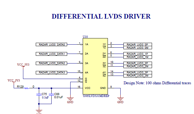
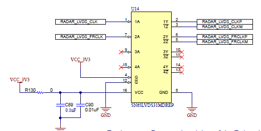
XWRL6432 doesn’t have LVDS I/Os, mainly to reduce the overall power consumption of the SOC. However, DCA1000 board needs LVDS signals on the clock and data interface for raw ADC capture so CMOS to LVDS converters are used on the board as shown below. Data capture interface uses RDIF (Radar Data interface) for transferring the data between mmWave device and DCA1000 capture card. There is no change needed in the DCA1000 capture card for this purpose, however a new low power mmWave studio need to be used for this purpose. Low power mmWave studio interpret the RDIF interface and provides the raw ADC data visualization platform for further signal processing.
 Figure 6-20 DCA1000 CMOS TO LVDS Conversation for Data Lines
 Figure 6-21 DCA1000 CMOS TO LVDS Conversation for Clock and Control Lines