SWRU596 December 2022
- 1Abstract
- 2Getting Started
- 3Hardware
- 4EVM Mux Block Diagram
- 5PCB Storage and Handling Recommendations:
- 6XWRL6432BOOST Antenna
- 7Software, Development Tools, and Example Code
- 8TI E2E Community
- 9References
6.2 Switch Settings
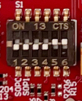
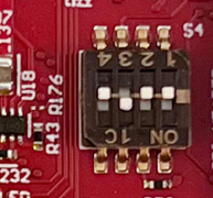
Figure 6-5 shows the part designators and positions of the switches (S1 and S4) on the XWRL6432BOOST.
 Figure 6-5 S1 Switch for Various Mode Settings
 Figure 6-6 S4 Switch for Various mode Settings
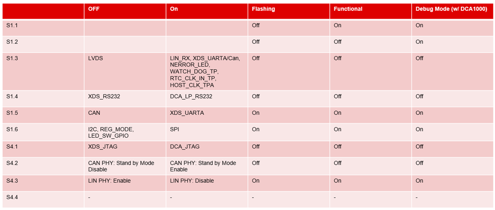
Figure 6-7 provides the different boot mode configurations to the device. Device supports application mode, QSPI flashing mode (Device management mode), and debug modes. This mode (SOP) configuration shown below in Figure 6-7 must be exercised first. After the SOP settings nRESET need to be issued to register the SOP settings. Figure 6-7 also provides the switch position for different modes of operation supported by the device and EVM.
 Figure 6-7 SOP Switches